Method for making a planar membrane
a planar membrane and membrane technology, applied in the direction of microstructured technology, material strength using tensile/compressive forces, decorative arts, etc., can solve the problem that the rigidity of the membrane is no longer sufficient to counter the weight effect, and achieve the effect of greater stack thermal expansion coefficient (soi)
- Summary
- Abstract
- Description
- Claims
- Application Information
AI Technical Summary
Problems solved by technology
Method used
Image
Examples
first embodiment
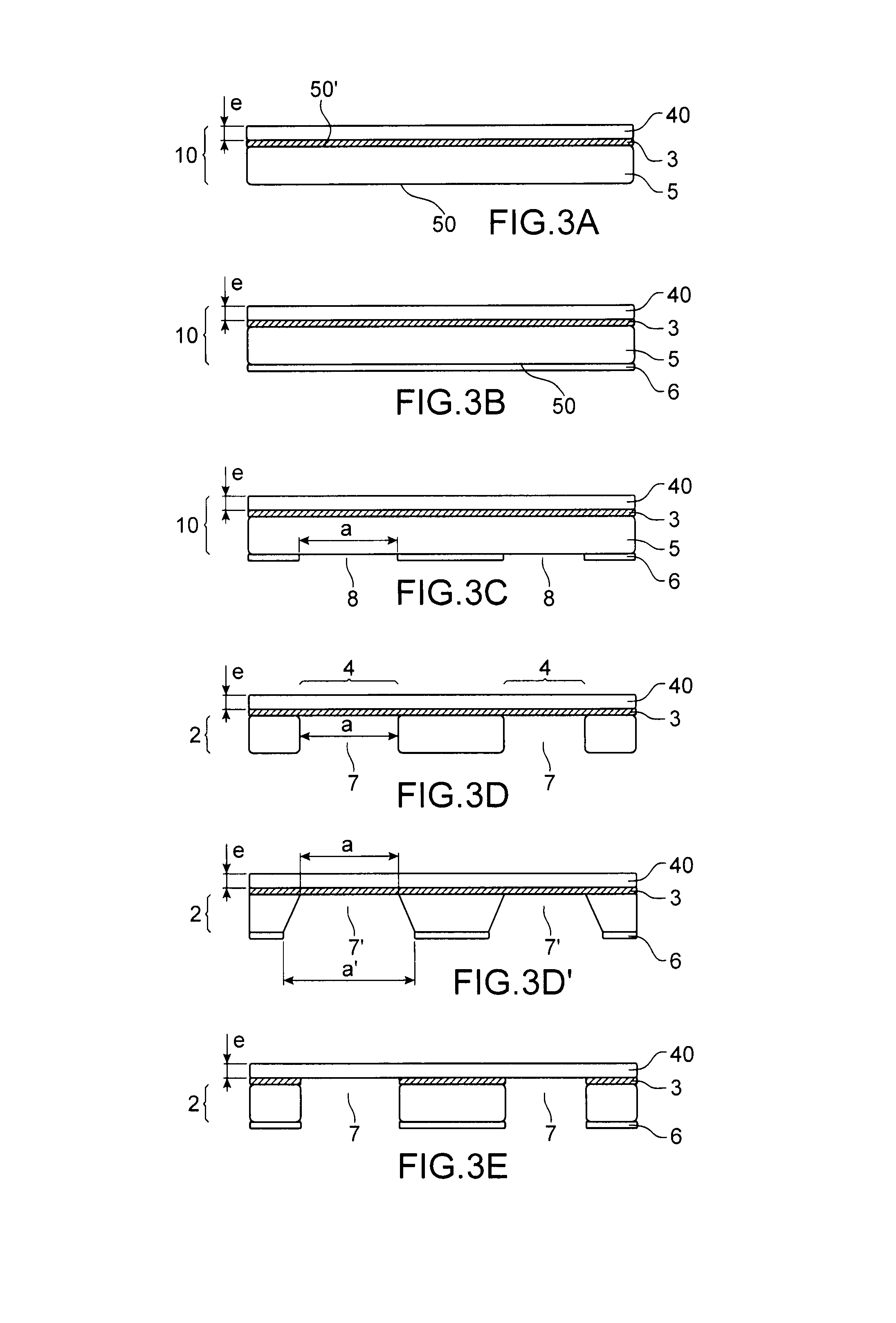
[0112]In the method of the invention, the deflection imposed to the membrane due to its own weight will be countered by the compensation stress formed by the initially present stress in the thin layer 40 of the sSOI substrate 10 which will give the membrane 4.
[0113]However, because of the method for forming the sSOI substrate 10, the layer in insulating material is generally subject to a compressive stress σoxide. This compressive stress σoxide, may be due to interface and edge effects. It may have a large value of more than 10 MPa, and even larger, or even larger than 1 GPa. A standard value is for example 300 MPa.
[0114]Thus, in the method according to the invention according to the first embodiment, in order that the minimum tension compensation stress in the membrane verifies equation (2), the existing compressive constraint σoxide existing in the layer of insulating material 3 and being found at the interface with the thin layer 40 is compensated. Therefore the initial tensile ...
second embodiment
[0131]In the method according to the invention, the aperture 7 advantageously crosses entirely the additional substrate 20 (FIG. 4C). At one at least of the main faces of the additional substrate 20, whether the piercing is isotropic or not, the aperture 7 has two dimensions a and b which are those selected during the method for determining the minimum tension compensation stress, since they correspond to the dimensions a and b of the membrane which is being formed. Said face of the additional substrate 20, referenced as 20.1, meeting this condition will then be designated as the active face 20.1 of the frame 2.
[0132]The material having been used as a mask, either the mask material 6, or the resin layer, may then be removed (FIG. 4D1). In the case when the mask material is present on the active face 20.1 of the frame 2, this material layer is necessarily removed after etching the aperture 7. FIG. 4C illustrates this configuration.
[0133]The piercing step may be followed by a step for...
PUM
| Property | Measurement | Unit |
|---|---|---|
| thickness | aaaaa | aaaaa |
| thickness | aaaaa | aaaaa |
| thickness | aaaaa | aaaaa |
Abstract
Description
Claims
Application Information
 - R&D
- Intellectual Property
- Life Sciences
- Materials
- Tech Scout
- Unparalleled Data Quality
- Higher Quality Content
- 60% Fewer Hallucinations
Browse by: Latest US Patents, China's latest patents, Technical Efficacy Thesaurus, Application Domain, Technology Topic, Popular Technical Reports.
© 2025 PatSnap. All rights reserved.Legal|Privacy policy|Modern Slavery Act Transparency Statement|Sitemap|About US| Contact US: help@patsnap.com


