Liquid crystal display device
a liquid crystal display and display screen technology, applied in the field can solve the problems of display defects, low alignment stability, and difficulty in adjusting the viewing angle of liquid crystal display devices, and achieve the effects of reducing the time constant of dc, improving the afterimage characteristics of photoalignment films, and improving the viscosity of varnishes
- Summary
- Abstract
- Description
- Claims
- Application Information
AI Technical Summary
Benefits of technology
Problems solved by technology
Method used
Image
Examples
embodiment 1
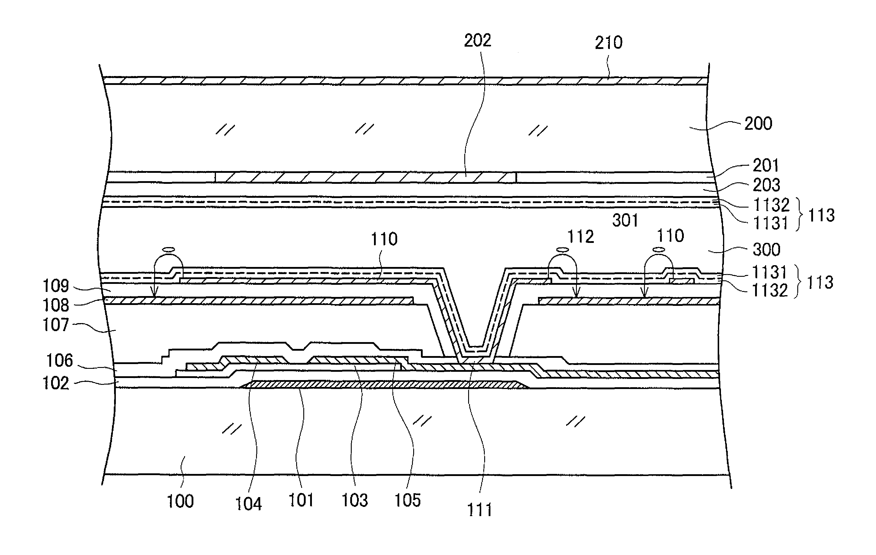
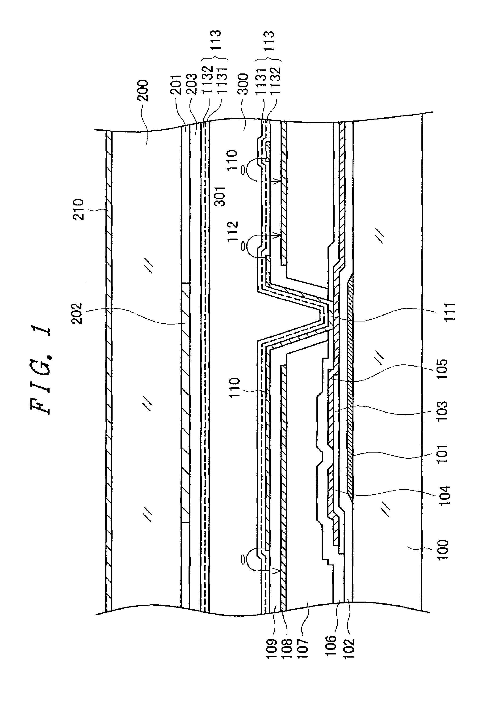
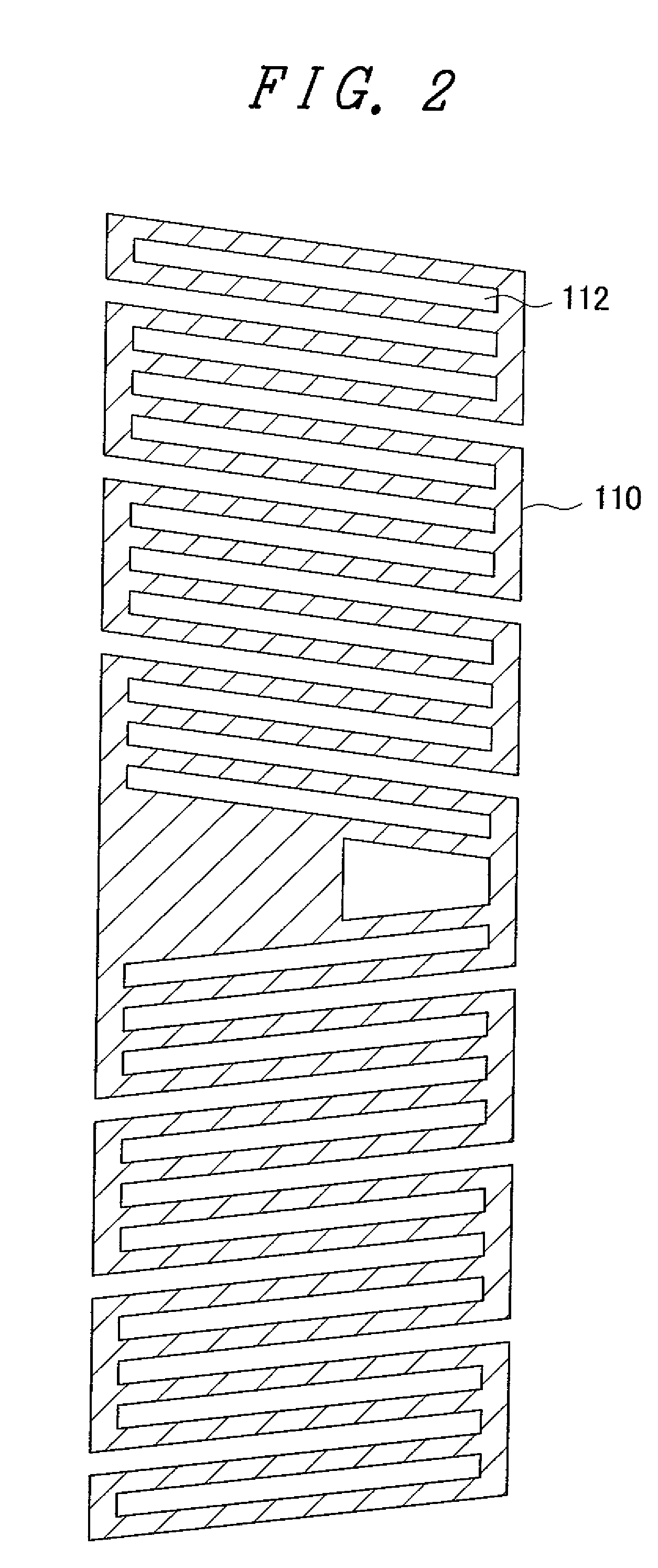
[0029]FIG. 1 is a cross-sectional diagram showing a structure in a display region of an IPS liquid crystal display device. Various structures are being proposed and put to practical use for the electrode structure of IPS liquid crystal display devices. The structure in FIG. 1 is a structure that is currently being widely used; simply put, a pectinate pixel electrode 110 is formed on an opposing electrode 108 formed in a flat solid, with an insulating film sandwiched between the pixel electrode 110 and the opposing electrode 108. Additionally, the liquid crystal display device forms an image by controlling the transmittance of light through a liquid crystal layer 300 per pixel by causing liquid crystal molecules 301 to be rotated by a voltage between the pixel electrodes 110 and the opposing electrodes 108. The structure in FIG. 1 will be described in detail below. It will be noted that, although the invention will be described taking the structure in FIG. 1 as an example, the invent...
embodiment 2
[0075]In embodiment 1, a film obtained by imidizing the polyamide acid is used as the low-resistivity alignment film 1132 on the bottom of the 2-layer alignment film 113. The low-resistivity alignment film 1132 has no relationship with photoalignment, so a material can be selected focusing on making the resistance of the alignment film 113 small.
[0076]In liquid crystal display devices, a backlight is disposed on the back surface of the liquid crystal display panel, and an image is formed by controlling the light from the backlight per pixel. A cold-cathode tube or a light-emitting diode is used as the light source of the backlight. Consequently, the alignment film 113 becomes always exposed to the light from the backlight while the liquid crystal display device is operating. When a photoconductive film is used as the low-resistivity alignment film 1132 on the bottom, the electric charge with which the liquid crystal layer has been charged can be let out more quickly, and DC afterima...
PUM
| Property | Measurement | Unit |
|---|---|---|
| thickness | aaaaa | aaaaa |
| thickness t2 | aaaaa | aaaaa |
| resistivity | aaaaa | aaaaa |
Abstract
Description
Claims
Application Information
 - R&D
- Intellectual Property
- Life Sciences
- Materials
- Tech Scout
- Unparalleled Data Quality
- Higher Quality Content
- 60% Fewer Hallucinations
Browse by: Latest US Patents, China's latest patents, Technical Efficacy Thesaurus, Application Domain, Technology Topic, Popular Technical Reports.
© 2025 PatSnap. All rights reserved.Legal|Privacy policy|Modern Slavery Act Transparency Statement|Sitemap|About US| Contact US: help@patsnap.com


