Electron emitting element, method for producing electron emitting element, electron emitting device, charging device, image forming apparatus, electron-beam curing device, light emitting device, image display device, air blowing device, and cooling device

a technology electron beam, which is applied in the field of electron emitting element, can solve the problems of oxidizing various substances, breaking down the element, and ozone being harmful to human bodies, and achieves the effects of reducing power consumption, efficient electron emission, and prolonging the life of the electron emitting elemen

Active Publication Date: 2013-07-16
SHARP KK
View PDF116 Cites 5 Cited by
  • Summary
  • Abstract
  • Description
  • Claims
  • Application Information

AI Technical Summary

Benefits of technology

[0016]According to the arrangement, the application of the voltage between the electrode substrate and the thin-film electrode generates a current path on an interface between the crystalline electron transport agent crystallized in the electron acceleration layer and fine particles in the electron acceleration layer. A part of an electric charge conducted in the current path becomes ballistic electrons due to an intense electric field formed by the applied voltage. The ballistic electrons are emitted from the thin-film electrode.
[0017]It is considered that (i) an electric property of a crystal grain boundary depends on consistency of a grain boundary and / or consistency of an interface, and (ii) the higher such consistency is, the lower an electrostatic potential barrier is in height. Therefore, according to the arrangement described above, it is considered that the electric charge can be conducted via a low electric potential barrier part, which is formed by the crystallization of the crystalline electron transport agent. That is, it becomes possible to form a current path with an applied voltage lower than an applied voltage of a conventional element.
[0018]Accordingly, in the arrangement in which the crystalline electron transport agent is crystallized in the electron acceleration layer, it is possible to emit electrons in an amount equal to or more than an amount with the conventional element, with an applied voltage lower than that of the conventional element. Such a reduction in the applied voltage can lead to extension of a lifetime of the electron emitting element, a reduction in power consumption, etc. Further, it becomes possible to provide the electron emitting element which can efficiently emit electrons, at low cost, without using an expensive material for the electron acceleration layer.
[0019]Here, a mechanism for generating ballistic electrons in the electron acceleration layer has a lot of unexplained points. However, is considered that the ballistic electrons are emitted from a surface of the electron emitting element in the following manner. A part of the electric charge conducted through the current path formed in the electron acceleration layer is accelerated due to an intense electric field which is locally formed, so as to be hot electrons (ballistic electrons). The hot electrons move along the electric field formed in the electron acceleration layer while being subjected to elastic collision repeatedly. A part of the hot electrons are transmitted trough the thin-film electrode serving as a surface of the electron emitting element, or passes thorough gaps of the thin-film electrode, so as to be emitted from the surface of the electron emitting element.
[0020]Further, an amount of the crystalline electron transport agent, used in the formation of the electron acceleration layer, should be set appropriately for the following reasons: (i) an excess amount of the crystalline electron transport agent added to the dispersion solution causes a current to flow so easily that it becomes impossible to apply a voltage necessary for the electron emission; (ii) on the other hand, an insufficient amount of the crystalline electron transport agent added to the dispersion solution makes it impossible to obtain a sufficient amount of a current, so that it becomes impossible to emit electrons. An appropriate amount of the crystalline electron transport agent should be set in accordance with parameters related to a resistance value of the electron emitting element (e.g. an amount of the conductive fine particles to be added, a layer thickness of the electron acceleration layer, and a film thickness of the resistance layer (later described)). Appropriate adjustment of the amount of the crystalline electron transport agent allows the electron emitting element to emit electrons sufficiently.

Problems solved by technology

This causes a problem of breakdown of the element due to sputtering.
Ozone is harmful to human bodies, and oxidizes various substances because of its strong oxidizing power.
This causes a problem in that members around the element are damaged.
In order to prevent this problem, the members used around the electron emitting element are limited to members that have high resistance to ozone.

Method used


Image

  • Electron emitting element, method for producing electron emitting element, electron emitting device, charging device, image forming apparatus, electron-beam curing device, light emitting device, image display device, air blowing device, and cooling device
  • Electron emitting element, method for producing electron emitting element, electron emitting device, charging device, image forming apparatus, electron-beam curing device, light emitting device, image display device, air blowing device, and cooling device
  • Electron emitting element, method for producing electron emitting element, electron emitting device, charging device, image forming apparatus, electron-beam curing device, light emitting device, image display device, air blowing device, and cooling device

Examples


embodiment 1

(Arrangements of Electron Emitting Element and Electron Emitting Device)

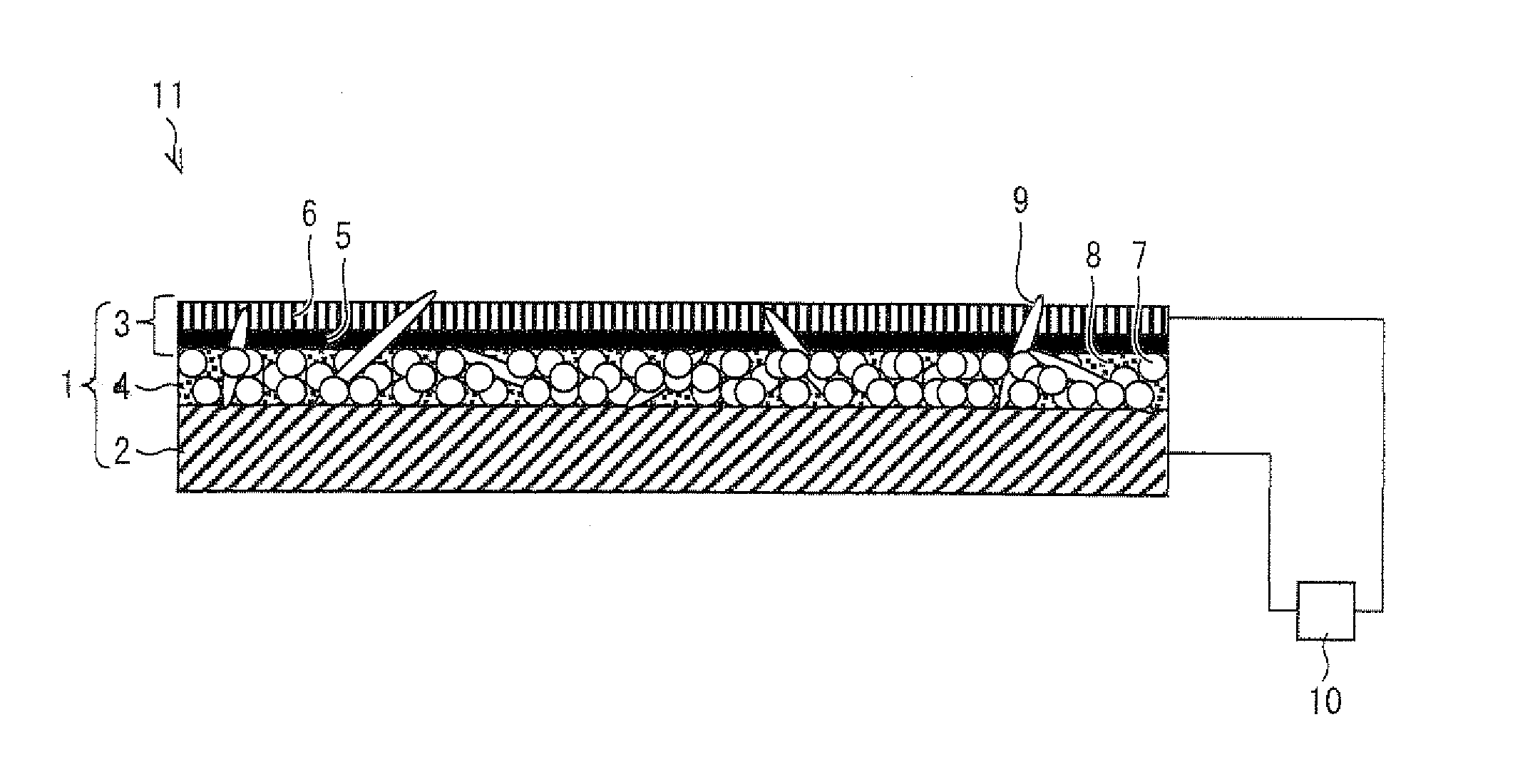
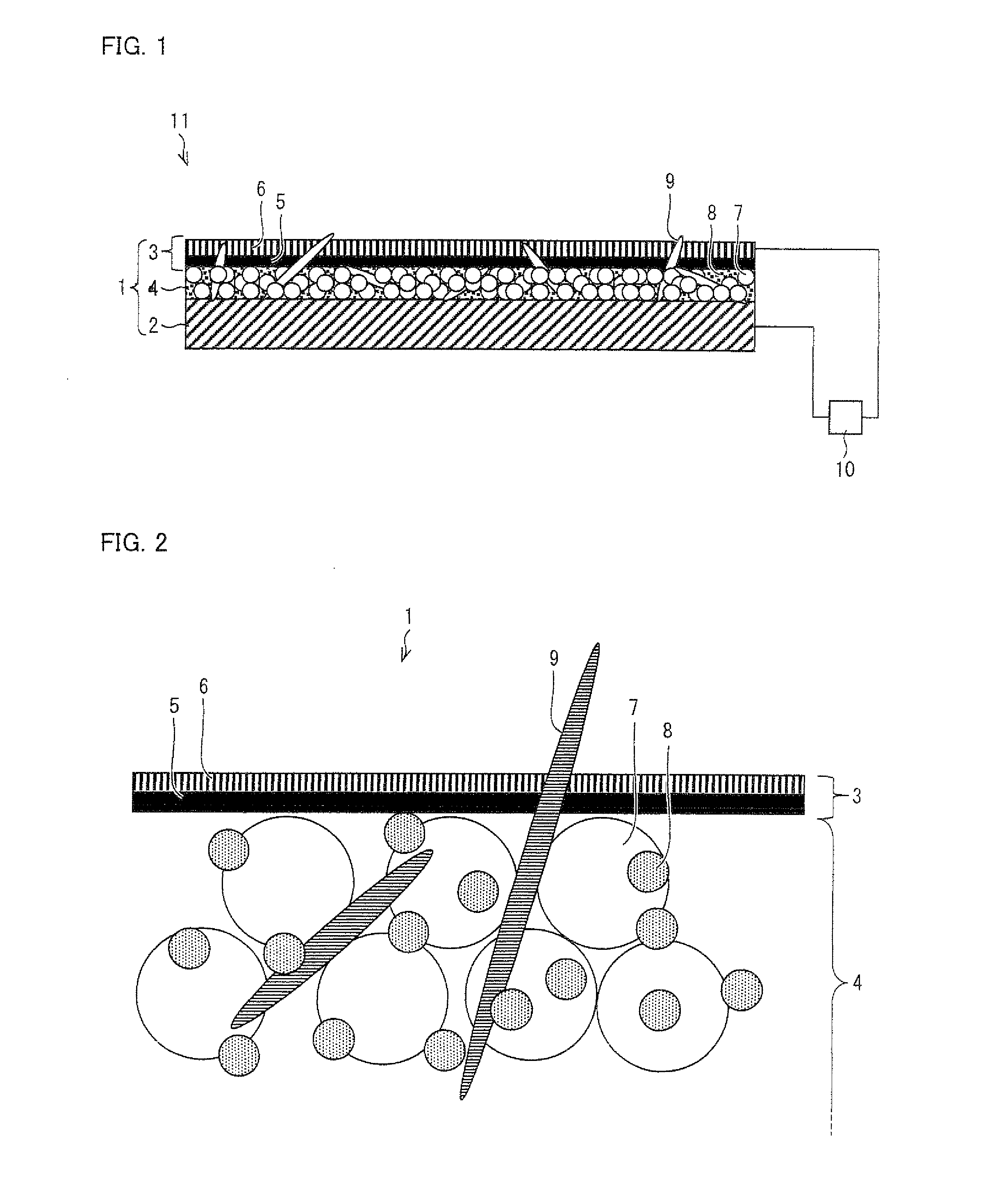
[0043]FIG. 1 is a view schematically illustrating an arrangement of an electron emitting device 11 employing an electron emitting element 1 in accordance with one embodiment of the present invention. The electron emitting device 11 includes the electron emitting element 1 of the embodiment of the present invention, and a power supply 10 (see FIG. 1). The electron emitting element 1 includes an electrode substrate 2 serving as a lower electrode, a thin-film electrode 3 serving as an upper electrode, and an electron acceleration layer 4 sandwiched between the electrode substrate 2 and the thin-film electrode 3. Further, the electrode substrate 2 and the thin-film electrode 3 are connected to the power supply (power supply section) 10, so that a voltage can be applied between the electrode substrate 2 and the thin-film electrode 3 which are provided so as to face each other. The electron emitting element 1 applies ...

example

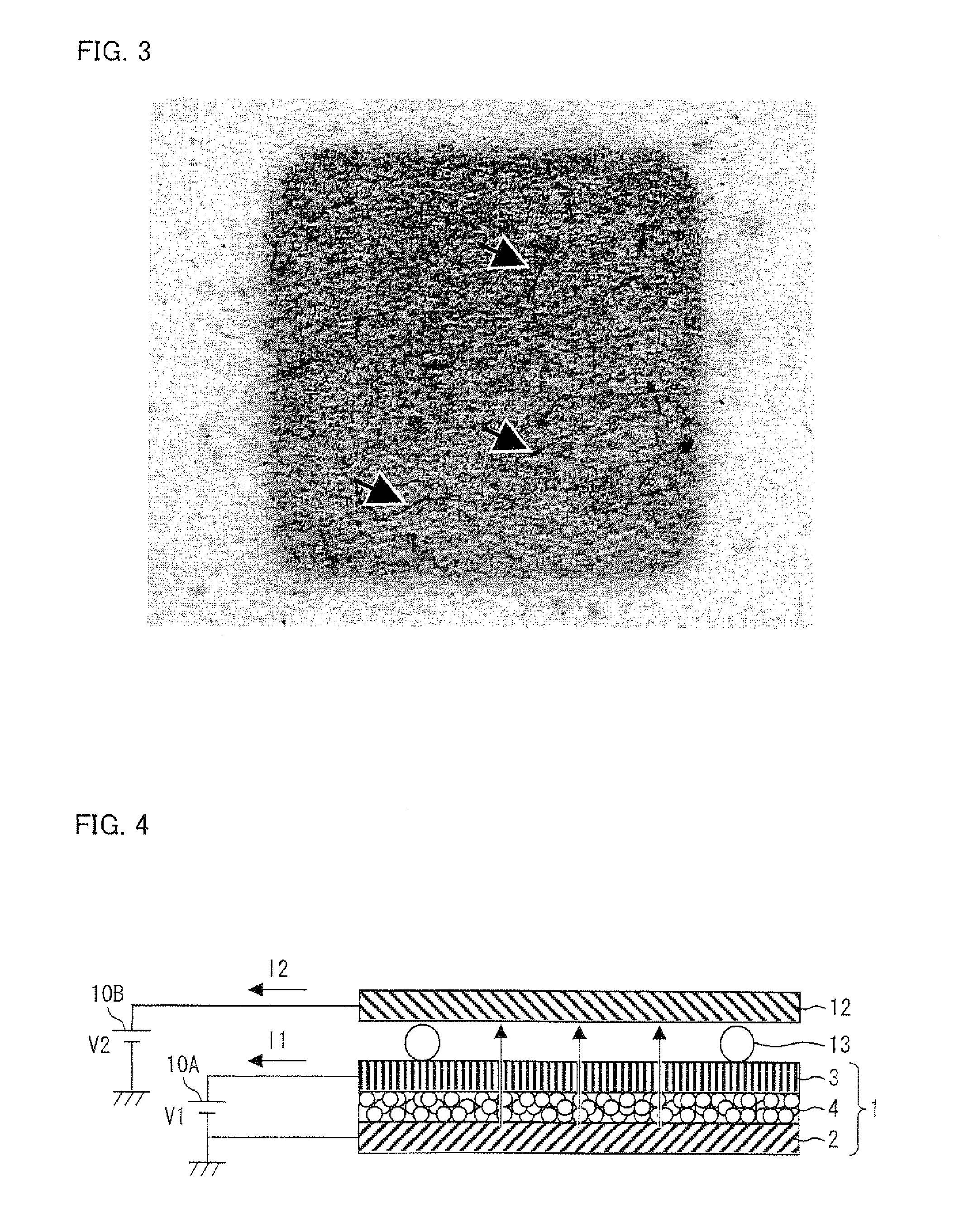
[0078]In the following Example, first, the descriptions deal with a result of an experiment for finding (i) how the current in the electron emitting element 1 changes as the amount of the crystalline electron transport agent 9 to be added is changed, and (ii) how the amount of emitted electrons changes as the amount of the crystalline electron transport agent 9 to be added is changed, in a case where the crystalline electron transport agent 9 is in an amorphous state in the electron acceleration layer 4 (the crystalline electron transport agent 9 has not been crystallized). Secondly, the descriptions deal with a result of measurement of (i) the current in the electron emitting element 1 and (ii) the amount of emitted electrons, which measurement was carried out for each of (i) the electron emitting element 1 in which the crystalline electron transport agent 9 was in the amorphous state, and (ii) the electron emitting element 1 in which the crystalline electron transport agent 9 had ...

embodiment 2

[0097]FIG. 14 shows an example of a charging device 90 of the present invention, including an electron emitting device 11 employing an electron emitting element 1 in accordance with an embodiment of the present invention, which electron emitting element 1 is described in Embodiment 1.

[0098]The charging device 90 includes the electron emitting device 11 including the electron emitting element and a power supply 10 for applying a voltage to the electron emitting element 1. The charging device90 is used for electrically charging a photoreceptor drum 14. An image forming apparatus of the present invention includes the charging device 90.

[0099]In the image forming apparatus of the present invention, the electron emitting element 1 in the charging device 90 is provided so as to face the photoreceptor drum 14 to be charged. Application of a voltage causes the electron emitting element 1 to emit electrons so that the photoreceptor drum 14 is electrically charged. In the image forming appara...


PUM


Abstract

An electron emitting element of the present invention includes: an electrode substrate; a thin-film electrode; and an electron acceleration layer sandwiched between the electrode substrate and the thin-film electrode, the electron acceleration layer including (i) conductive fine particles, (ii) insulating fine particles having an average particle diameter greater than an average particle diameter of the conductive fine particles, and (iii) a crystalline electron transport agent. The crystalline electron transport agent is crystallized in the acceleration layer.

Description

[0001]This Nonprovisional application claims priority under 35 U.S.C. §119(a) on Patent Application No. 2009-273724 filed in Japan on Dec. 1, 2009, the entire contents of which are hereby incorporated by reference.TECHNICAL FIELD[0002]The present invention relates to an electron emitting element for emitting electrons by application of a voltage, and a method for producing the electron emitting element. The present invention further relates to: an electron emitting device; a charging device; an image forming apparatus; an electron-beam curing device; a light emitting device; an image display device; an air blowing device; and a cooling device, each of which includes the electron emitting element.BACKGROUND ART[0003]A Spindt-type electrode and a carbon nanotube electrode (CNT) have been known as conventional electron emitting elements. Applications of such conventional electron emitting elements to, for example, the field of Field Emission Display (FED) have been studied. Such electr...

Claims


Application Information

Patent Timeline
Patent Type & Authority Patents(United States)
IPC IPC(8): H01J1/00
CPCH01J63/06G03G15/02H01J2329/0434
Inventor HIRAKAWA, HIROYUKIIMURA, YASUO
Owner SHARP KK
Why Eureka
Try Eureka