Top tri-metal system for silicon power semiconductor devices

a technology of silicon power semiconductor devices and top metal systems, which is applied in the direction of layered products, transportation and packaging, chemical instruments and processes, etc., can solve the problems of corroding and compromising the solder connection, and achieve the effect of avoiding the high cost of gold and the corrosion tendency of silver without compromising performance, less wafer rejection, and less prone to scratching

Inactive Publication Date: 2013-04-23
DIODES INC
View PDF11 Cites 0 Cited by
  • Summary
  • Abstract
  • Description
  • Claims
  • Application Information

AI Technical Summary

Benefits of technology

[0007]The present invention provides a number of advantages over prior art metal systems. For example, the use of palladium avoids the high cost of gold and the corrosion tendency of silver without compromising performance. Furthermore, palladium is harder (approximately 4.75 on the Mohs scale) and less prone to scratching than gold or silver and, therefore, results in fewer wafer rejections. Additionally, where the electrodes are exposed to multiple iterations of the soldering cycle, palladium, unlike gold, will not interact with and allow the nickel to migrate to the outer surface of the metal system where it may corrode and compromise the soldered connection.

Problems solved by technology

Additionally, where the electrodes are exposed to multiple iterations of the soldering cycle, palladium, unlike gold, will not interact with and allow the nickel to migrate to the outer surface of the metal system where it may corrode and compromise the soldered connection.

Method used


Image

  • Top tri-metal system for silicon power semiconductor devices
  • Top tri-metal system for silicon power semiconductor devices
  • Top tri-metal system for silicon power semiconductor devices

Examples


Embodiment Construction

.

BRIEF DESCRIPTION OF THE DRAWING FIGURES

[0009]The present invention is described herein with reference to the following drawing figures, which are not necessarily to actual scale:

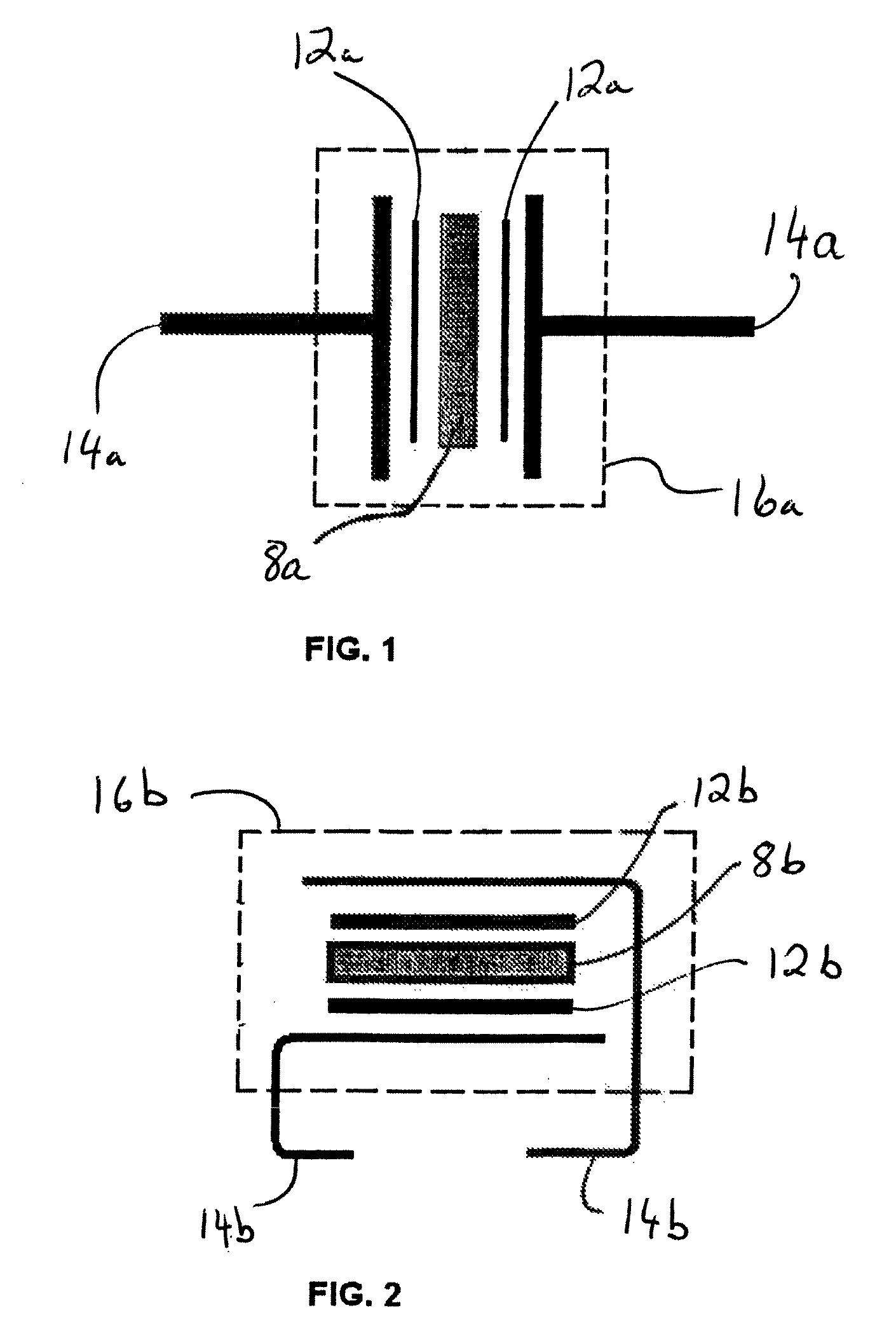
[0010]FIG. 1 is a representation of a semiconductor chip packaged in an axial configuration;

[0011]FIG. 2 is a representation of a semiconductor chip packaged in a surface-mounted configuration;

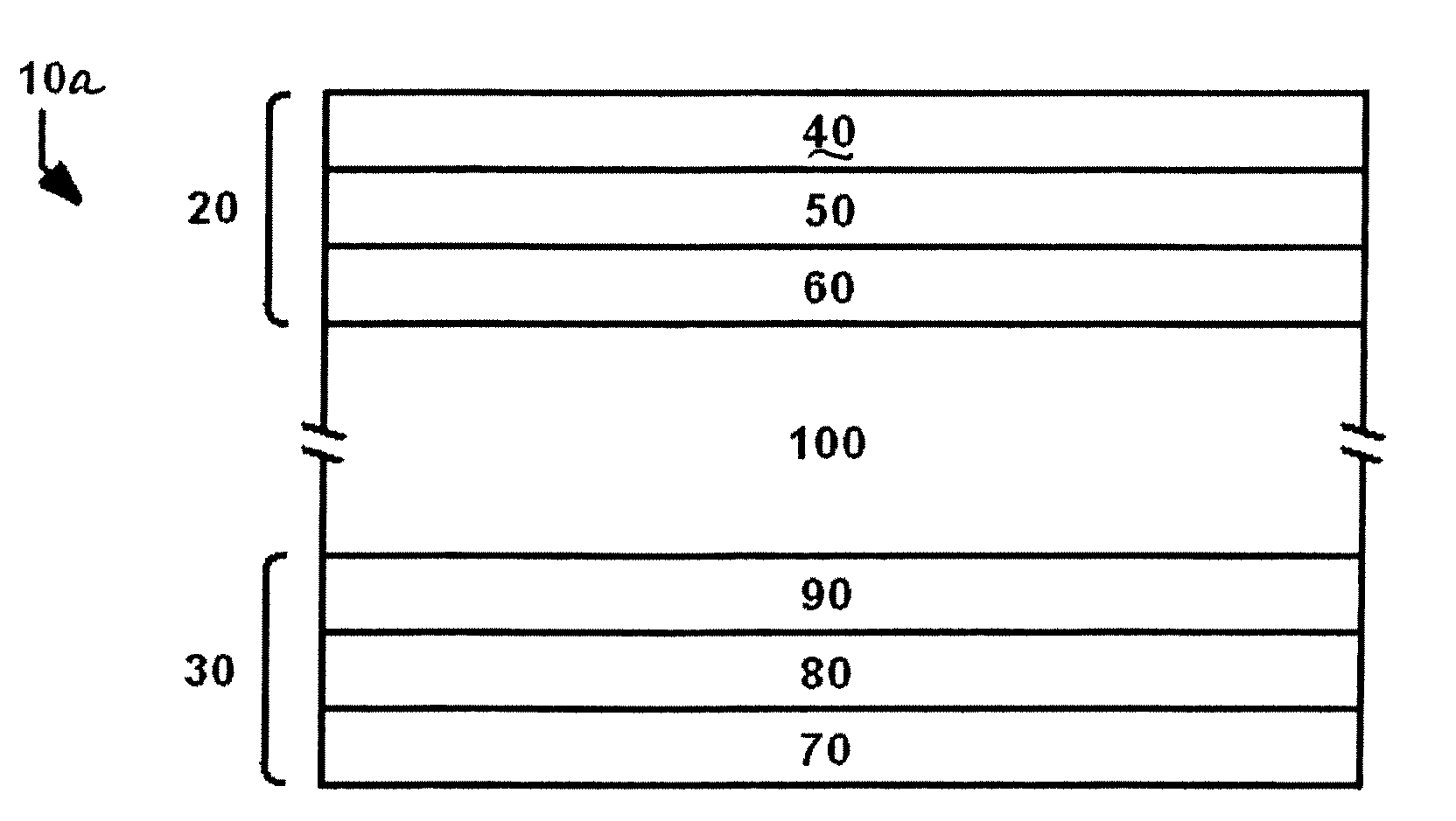
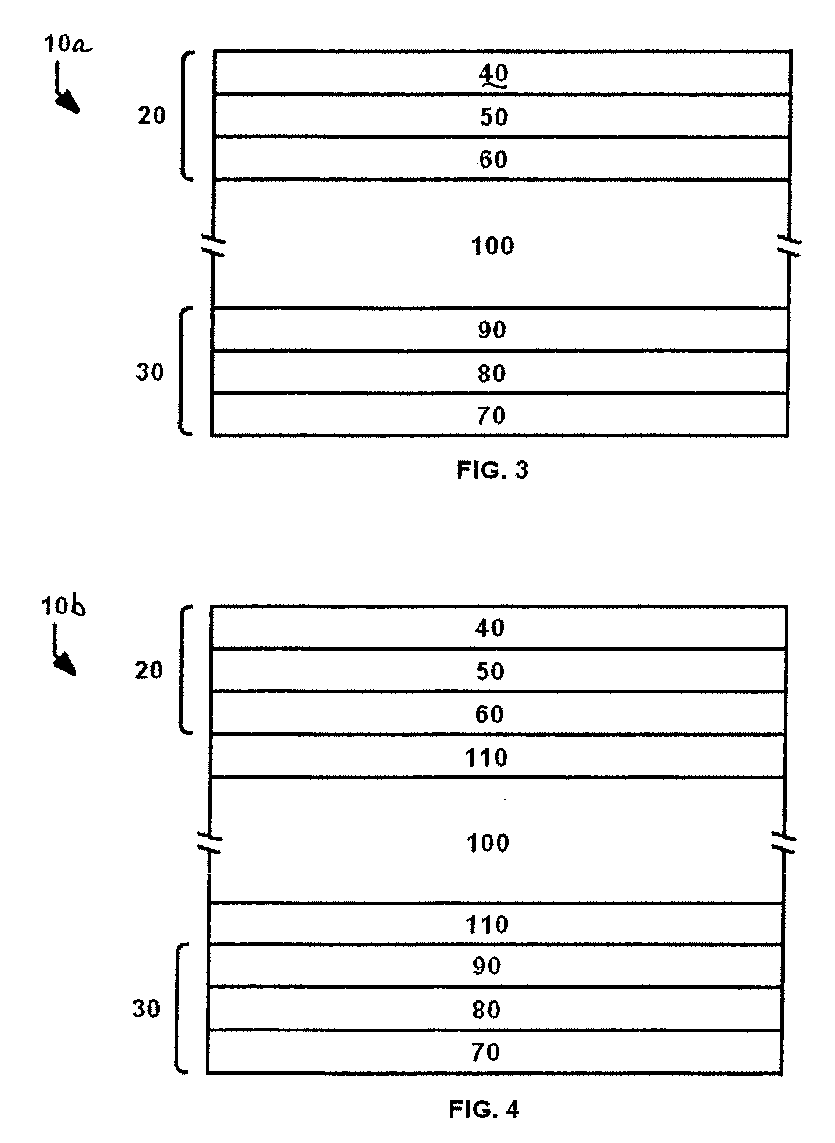
[0012]FIG. 3 is a schematic cross-sectional elevation view representation of a power semiconductor device including the top metal system of the present invention deposited on silicon; and

[0013]FIG. 4 is a schematic cross-sectional elevation view representation of a power semiconductor device including the top metal system of the present invention deposited on one or more additional metals.

DETAILED DESCRIPTION OF THE INVENTION

[0014]With reference to the drawings figures, a metal system for power semiconductor devices is herein described, shown, and otherwise disclosed in accordance with various embodiments, including ...


PUM

PropertyMeasurementUnit
thicknessaaaaaaaaaa
thicknessaaaaaaaaaa
thicknessaaaaaaaaaa

Abstract

A titanium-nickel-palladium solderable metal system for silicon power semiconductor devices (10), which may be used for one or both of the anode (20) or cathode (30). The metal system includes an outer layer of palladium (40,70), an intermediate layer of nickel (50,80), and an inner layer of titanium (60,90). For certain applications, the nickel may be alloyed with vanadium. The metal system may be deposited on bare silicon (100) or on one or more additional layers of metal (110) which may include aluminum, aluminum having approximately 1% silicon, or metal silicide. The use of palladium, rather than gold or silver, reduces cost, corrosion, and scratching.

Description

FIELD OF THE INVENTION[0001]The present invention relates broadly to top metal systems for power semiconductor devices. More specifically, the present invention concerns titanium-nickel-palladium top metal systems for silicon power semiconductor devices.BACKGROUND[0002]Discrete (non-integrated) power semiconductor devices are often built using a vertical structure in which electrical current passes through the thickness of the chip between the front and back surfaces of the device. The front surface of such devices presents an anode or “front metal,” the back surface presents a cathode or “back metal,” and each electrode takes the form of a metal pad comprising several layers of metal. Alternatively, the front surface presents the cathode, and the back surface presents the anode. Because these metal layers are deposited on top of any other layers, both front metal and back metal are often referred to herein as “top metal.” Some devices present more than one electrode on one or both ...

Claims


Application Information

Patent Timeline
Patent Type & Authority Patents(United States)
IPC IPC(8): H01L23/48H01L23/52H01L29/40
CPCH01L29/456H01L24/01H01L2924/13091Y10T428/12743H01L2924/1305Y10T428/12806H01L2924/00H01L2924/12032H01L2924/12036H01L2924/12041
Inventor HAMERSKI, ROMAN
Owner DIODES INC
Why Eureka
Try Eureka