Wiring substrate and method for manufacturing wiring substrate

a wiring substrate and manufacturing method technology, applied in the field of wiring substrates, can solve the problems of decrease achieve the effects of reducing the insulation resistance reducing the warping and bending degrees, and low strength of such a wiring substra

Active Publication Date: 2013-04-16
IBIDEN CO LTD
View PDF6 Cites 0 Cited by
  • Summary
  • Abstract
  • Description
  • Claims
  • Application Information

AI Technical Summary

Benefits of technology

[0003]However, since the insulative region of the core substrate in Patent Publication (1) has a porous region, if the core substrate in Patent Publication (1) is used as a wiring substrate, it is thought that the strength of such a wiring substrate will be low. Accordingly, it is assumed that the degrees of warping and bending may become greater in the wiring substrate. Also, it is assumed that water may seep into holes of the porous region, thus decreasing the insulation resistance of the wiring substrate.

Problems solved by technology

However, since the insulative region of the core substrate in Patent Publication (1) has a porous region, if the core substrate in Patent Publication (1) is used as a wiring substrate, it is thought that the strength of such a wiring substrate will be low.
Also, it is assumed that water may seep into holes of the porous region, thus decreasing the insulation resistance of the wiring substrate.

Method used


Image

  • Wiring substrate and method for manufacturing wiring substrate
  • Wiring substrate and method for manufacturing wiring substrate
  • Wiring substrate and method for manufacturing wiring substrate

Examples


embodiment

[Embodiment]

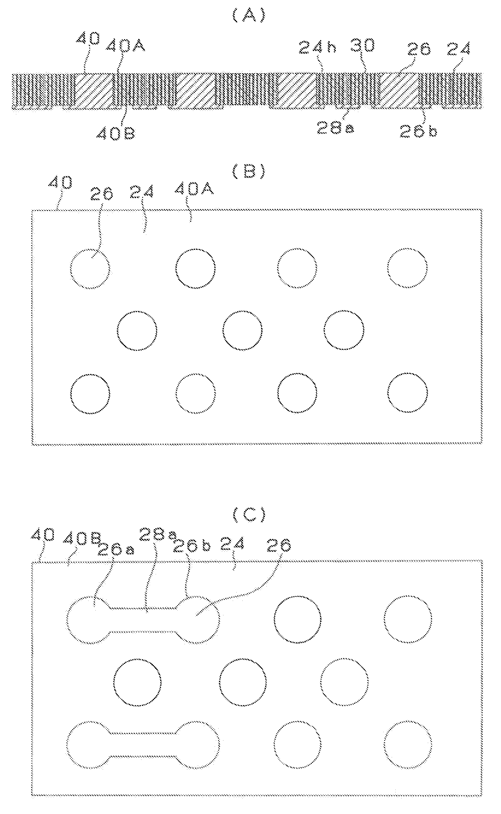
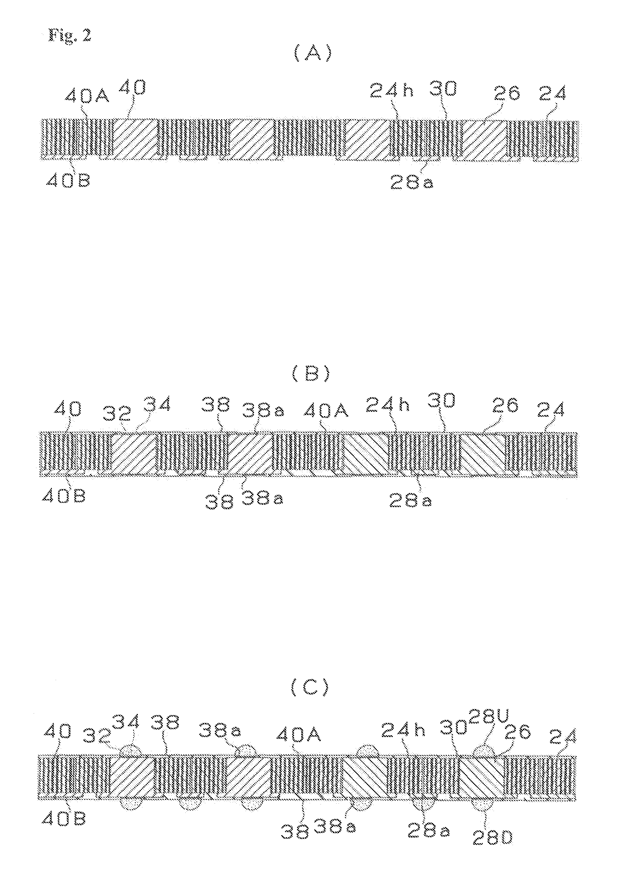
[0023]A method for manufacturing a wiring substrate according to an embodiment of the present invention is described with reference to the drawings. Metal plate 20 is prepared as a starting material (FIG. 1(A)). As for such a metal plate, the following may be listed: aluminum plate, magnesium plate, titanium plate, zinc plate, tantalum plate, niobium plate, hafnium plate, zirconium plate, tungsten plate, bismuth plate, antimony plate, aluminum alloy plate, titanium alloy plate and magnesium alloy plate. Since aluminum is a lightweight metal for use as a metal plate, it is suitable as a material for a wiring substrate. A metal plate has first surface (20A) and second surface (20B) opposite the first surface. Resist is formed on both surfaces of metal plate 20. By exposing to light and developing the resist formed on first surface (20A), resist (22U) for anodic oxidation is formed in portions to form through-hole conductors. Resist (22U) for anodic oxidation formed on firs...

first example

[0050]A method for manufacturing a wiring substrate according to the first example of the present invention is described with reference to the drawings. In the first example, 100 μm-thick aluminum plate 20 (made by Nippon Light Metal Co., Ltd., 99.99 or greater wt. % purity) is used as a starting material (FIG. 1(A)). The aluminum plate has a first surface and a second surface opposite the first surface. Resist (brand name: Photec H-6200, made by Hitachi Chemical Co., Ltd.) is formed on both surfaces of aluminum plate 20. By exposing to light and developing the resist formed on first surface (20A), resist (22U) for anodic oxidation is formed in portions to form through-hole conductors. Protective film (22D) formed on the second surface covers second surface (20B) (FIG. 1(B)).

[0051]In the following anodic oxidation bath 100, aluminum plate 20, where first resist pattern (22U) and protective film (22D) are formed, and platinum plate 108 are immersed (see FIG. 3). Using the aluminum pl...

second example

[0062]The second example is the same as the first example except for the amount to be anodic oxidized. In the second example, the amount to be anodic oxidized is greater than that in the first example. The thickness of aluminum oxide to be formed through anodic oxidation is 95 μm (the thickness of the aluminum layer=5 μm). Namely, the thickness of conductive circuits made from the aluminum formed on the second surface of insulative substrate 24 is 5 μm.


PUM

PropertyMeasurementUnit
thicknessaaaaaaaaaa
thicknessaaaaaaaaaa
thicknessaaaaaaaaaa

Abstract

[Subject Matter] To provide a method for manufacturing a wiring substrate where rigidity is enhanced in an insulative portion made by oxidizing aluminum.[Solution(s)] Aluminum oxide insulative portion 24 is formed on aluminum plate 20 as shown in FIG. 1(A) through anodic oxidation (FIG. 1(C)). Then, holes (nano-holes) (24h) in aluminum oxide 24 are filled with resin 30 (FIG. 1(E)). Accordingly, the rigidity (strength) of insulative portion 24 will be enhanced and cracking will not occur during heat cycles. Also, the insulation reliability of aluminum oxide will increase, and short circuiting may be prevented at through holes 26 (aluminum portions) separated by aluminum oxide 24.

Description

TECHNICAL FIELD[0001]The present invention relates to a wiring substrate having an insulative substrate made of a metal oxide and having a through-hole conductor that penetrates through the insulative substrate and is made of metal which forms the metal oxide, and to a method for manufacturing such a wiring substrate.BACKGROUND ART[0002]Patent Publication (1) discloses a method for forming a buildup layer on a core substrate having a conductive region and an insulative region. In Patent Publication (1), by oxidizing portions of aluminum, a core substrate is formed with aluminum (conductive region) and aluminum oxide (insulative region). In addition, Patent Publication (1) discloses that the insulative region of Patent Publication (1) is made up of a porous region and a non-porous region, and that the porous layer provides non-conductive features and the denser region works as a barrier layer which prevents the conductive region from being oxidized.[Prior Art Publication][Patent Publ...

Claims


Application Information

Patent Timeline
Patent Type & Authority Patents(United States)
IPC IPC(8): C25F3/14C25D11/02
CPCC25D1/04C25D11/026C25D11/02H05K1/0306H05K3/4038H05K3/4605C25D5/022H05K3/06H05K3/244H05K3/3484H05K2201/0116H05K2201/0209H05K2203/0315H05K2203/043H05K2203/1142H05K2203/1147H05K3/3485
Inventor NAKAI, TORUCHEN, LIYI
Owner IBIDEN CO LTD
Why Eureka
Try Eureka