Conductor/insulator/porous film-device and its use with the electrochemiluminescence-based analytical methods
a technology of porous film and electrochemiluminescence, which is applied in the field of analytical methods and devices, can solve the problems of not being applicable to certain market needs, too expensive, and general burden of need for fast, sensitive and quantitative diagnostic technologies, and achieves the effect of facilitating pretreatment of whole blood samples and being more practical in us
- Summary
- Abstract
- Description
- Claims
- Application Information
AI Technical Summary
Benefits of technology
Problems solved by technology
Method used
Image
Examples
example 1
Preparation of the Insulating Film-Coated Electrodes from Si-Wafers by Thermal Oxidization, Slicing and Coating with Antibody
[0057]The oxidation of Si wafers. The wafers (Si wafers: resistivity 0.01-0.023 Ωcm, p++ boron-doped, orientation , thickness 525+ / −25 μm, producer Okmetic Oyj) were washed the RCA washing generally used in industry and were placed into an oven at 700° C., where the atmosphere contained 95% nitrogen, and 5% oxygen. The temperature was increased to 850° C. and oxygen partial pressure was increased: 90% nitrogen, 10% oxygen and incubated for the desired time. The wafers were rinsed with pure nitrogen flow for 30 min. The temperature was degreased back to 700° C. in pure nitrogen and the wafers were removed from the oven.
[0058]The following results were obtained with different oxidation times:
[0059]
Oxidation time (min)Thickness (nm) 0 (*)2.666 153.418 303.936 404.171 604.852 805.5351206.3932008.07040011.442
[0060]The thickness was measured by an ellipsometer by th...
example 2
Heterogeneous CRP Immunoassay Exemplified with Standard Solutions and the Test Strip and Measuring Cell in Accordance with FIGS. 1 and2
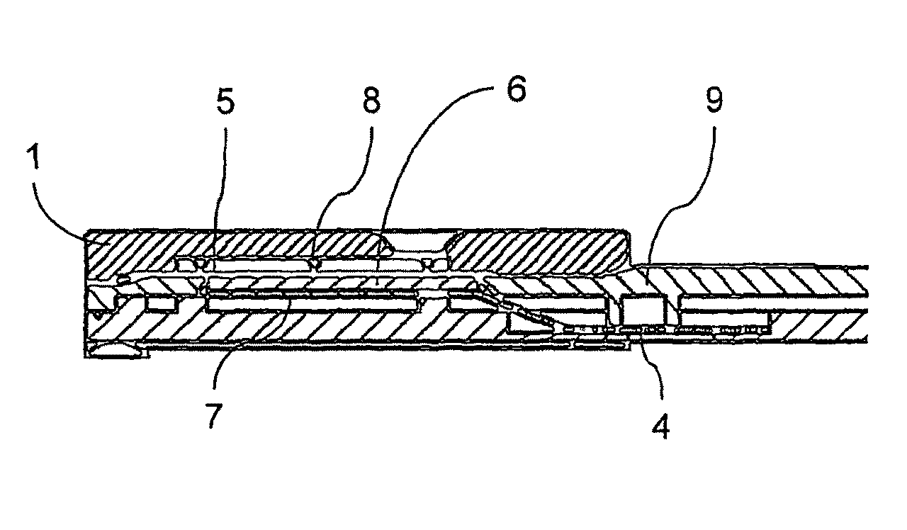
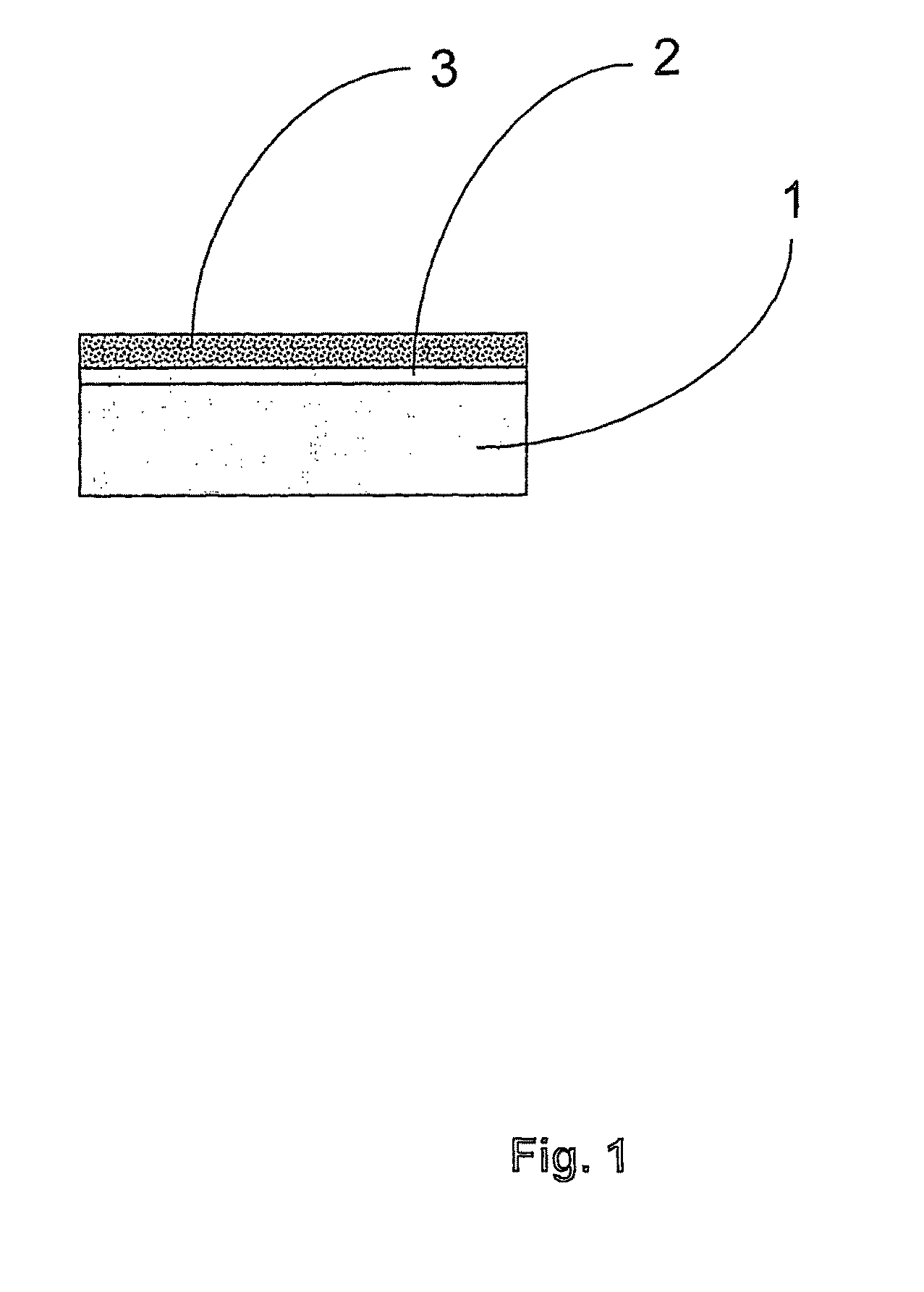
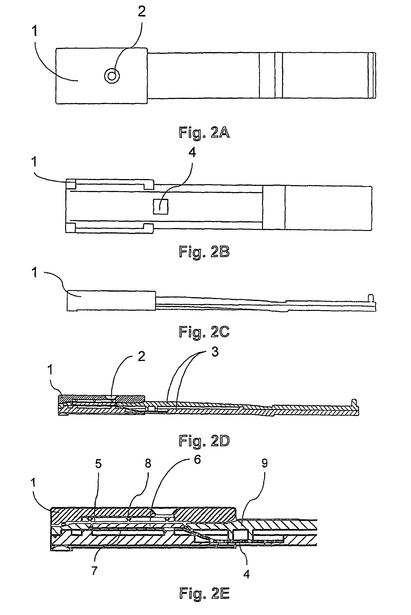
[0062]The CRP immunoassays were performed with Si-chips prepared according to Example 1. The construction of the test strips was as in FIG. 1 and FIG. 2. The sliding porous film-containing test strips were measured with the cell and device as shown in FIG. 3A. The immunoassay was based on the use of porous films combined with the ECL detection. Alternatively, by slightly modifying the test strip, it was possible to perform the measurement with the disposable measuring cell described in FIG. 3B.
[0063]Porous film attached to the sliding lid part of the test strip contained dried label. The polycarbonate porous film of outside measure of 7.00×12.0 mm (thickness 6-11 um, 1×10⁵-6×10⁸ holes / cm2, Whatman) was inserted to the tape frame of the same size (3M 465, two-sided acryl tape without backing material) having an opening of the size of Si chip 4.00×9.00...
example 3
Measurement of Tb-Chelate in the Measuring Cell Comprising of Anode Around Silicon Cathode
[0065]In the experimental arrangement of FIG. 5A the silicon electrode was attached with tape to the bottom of the well and was filled up to the surface with UV-polymerizing adhesive (Loctite 322 or EPO-TEK OG 142). After the polymerization the tape was removed. The cell was filled with the washing / measuring solution mentioned in Experiment 2, where the concentration of Tb chelate solution was 10−3 mol / l. ECL was measured (f=20 Hz, I=316 mM, pulsing time 500 μs, U=67 V) and photographs taken by a digital camera. Ten pulses were collected for obtaining the photograph. FIG. 5B shows that the luminescence is coming from the whole electrode area.
PUM
| Property | Measurement | Unit |
|---|---|---|
| thickness | aaaaa | aaaaa |
| thickness | aaaaa | aaaaa |
| thickness | aaaaa | aaaaa |
Abstract
Description
Claims
Application Information
 - R&D Engineer
- R&D Manager
- IP Professional
- Industry Leading Data Capabilities
- Powerful AI technology
- Patent DNA Extraction
Browse by: Latest US Patents, China's latest patents, Technical Efficacy Thesaurus, Application Domain, Technology Topic, Popular Technical Reports.
© 2024 PatSnap. All rights reserved.Legal|Privacy policy|Modern Slavery Act Transparency Statement|Sitemap|About US| Contact US: help@patsnap.com


