Method of making thin film transistor

a thin film transistor and transistor technology, applied in the field of thin film transistors, can solve the problems of increasing resistance and capacitor load, reducing and reducing the aperture, so as to achieve a larger turn-on current and reduce the channel length of the thin film transistor.

Active Publication Date: 2013-02-19
AU OPTRONICS CORP
View PDF5 Cites 0 Cited by
  • Summary
  • Abstract
  • Description
  • Claims
  • Application Information

AI Technical Summary

Benefits of technology

[0009]The photo-mask of the invention has the design of the transparent single slit and the translucent pattern. Therefore, the channel length of the thin film transistor can be reduced by the transparent single slit, and the extension portion of the semiconductor layer can be defined by the translucent pattern. As a result, the thin film transistor has a larger turn-on current.

Problems solved by technology

However, increasing the channel width of the thin film transistor may lead to some disadvantage, such as a lower aperture and an increasing load of resistances and capacitors.
On the other hand, decreasing the channel length of the thin film transistor may also enlarge the turn-on current.
But this method is difficult due to the limitation of the conventional photo-mask and the photolithographic process.

Method used


Image

  • Method of making thin film transistor
  • Method of making thin film transistor
  • Method of making thin film transistor

Examples


Embodiment Construction

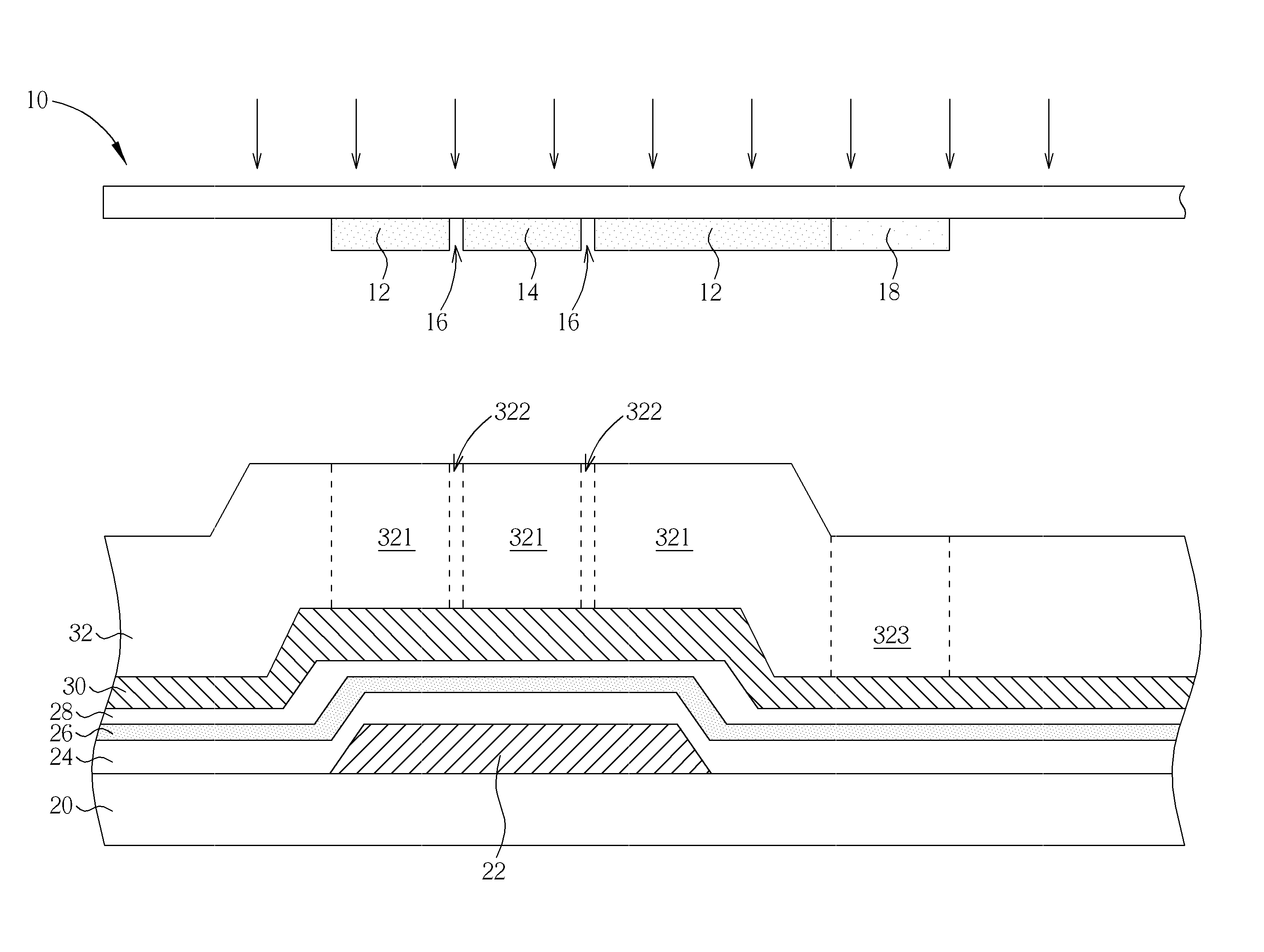
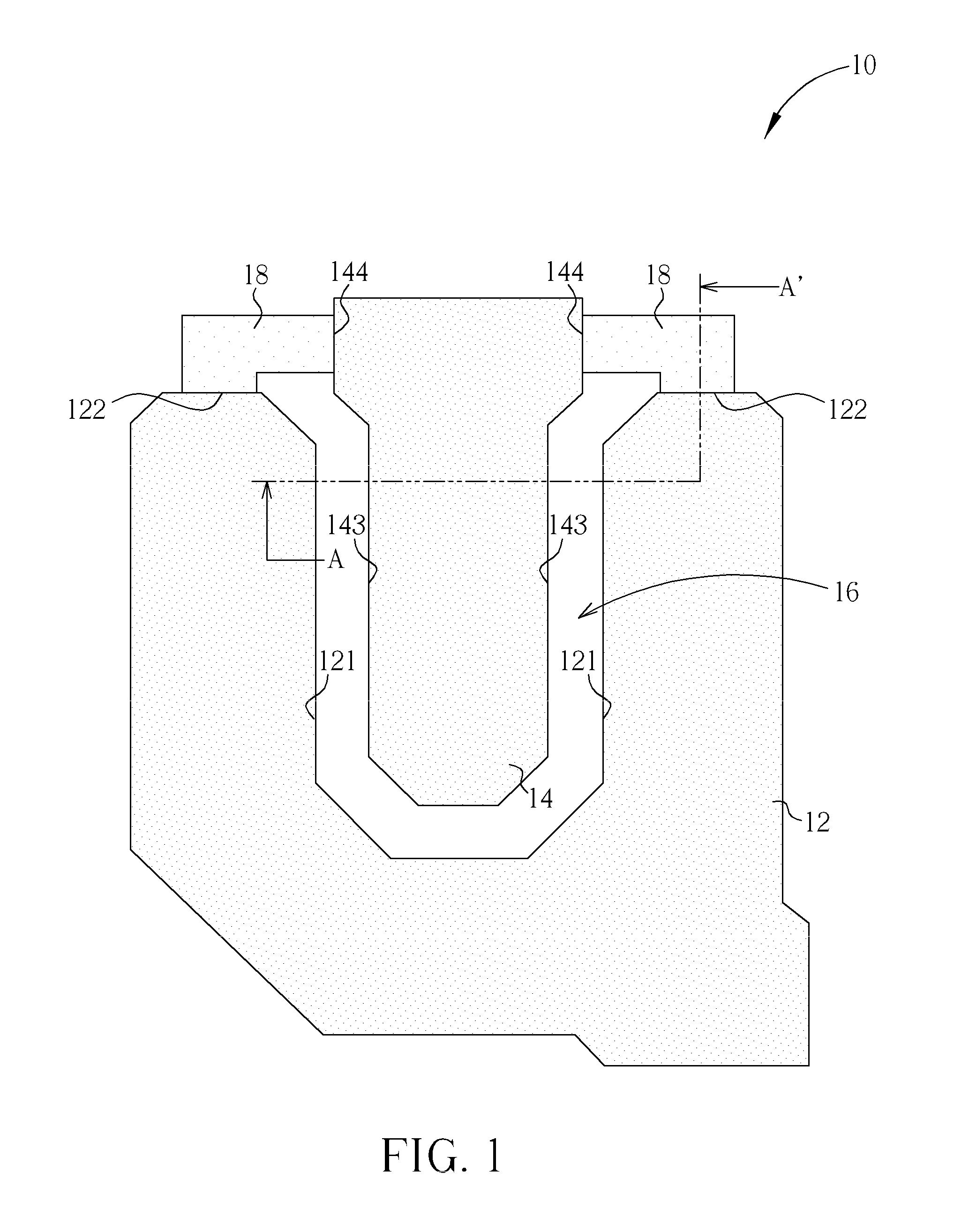
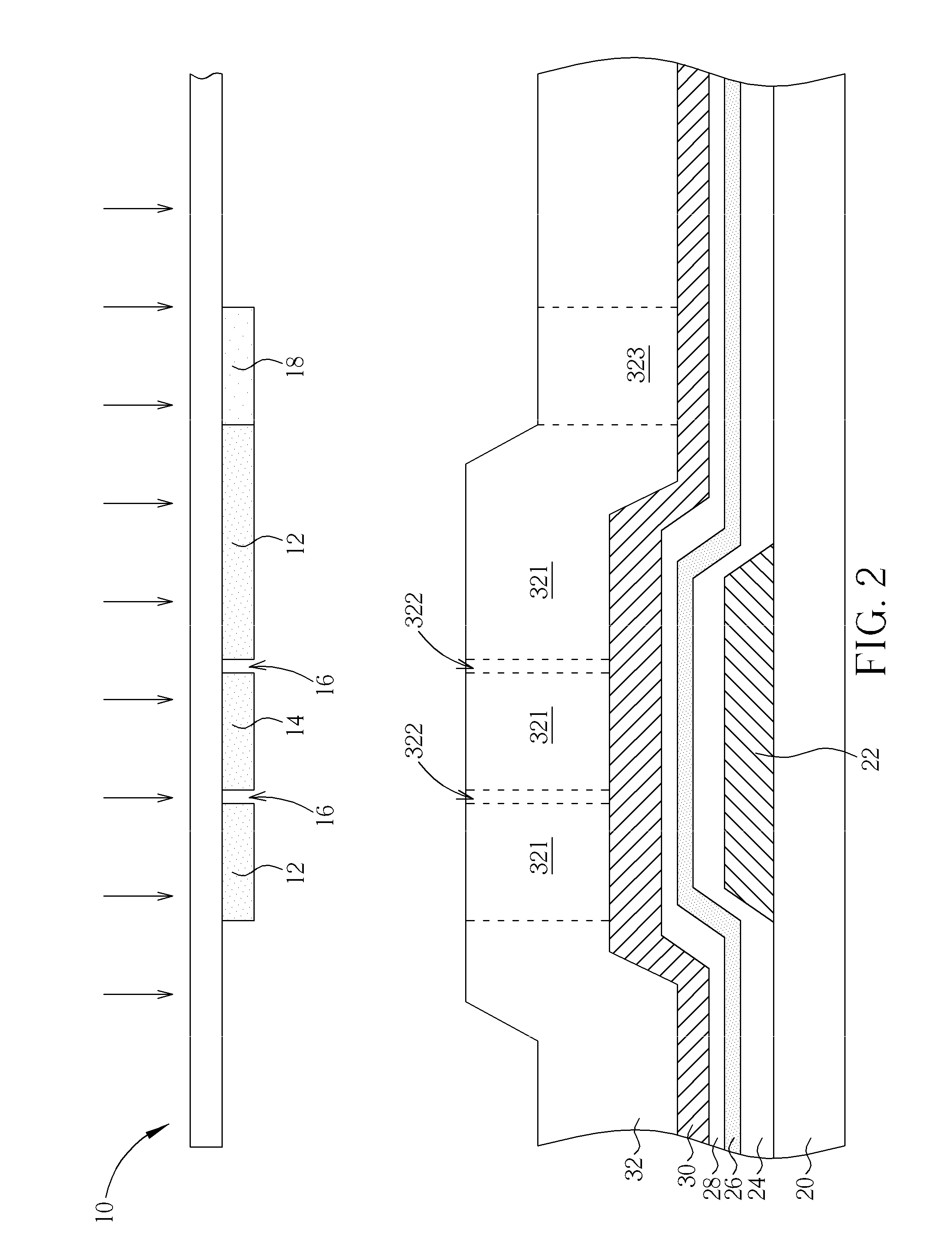
[0015]Please refer to FIG. 1. FIG. 1 schematically illustrates a photo-mask according to a preferred embodiment of the present invention. In this embodiment, the photo-mask 10 may be a graytone mask (GTM), a halftone mask (HTM), or other mask having different transmittance at different regions. The photo-mask 10 includes a first opaque pattern 12, a second opaque pattern 14, a transparent single slit 16, and a translucent pattern 18. The first opaque pattern 12 includes a first side edge 121 and a second side edge 122, the second opaque pattern 14 includes a third side edge 143 and a fourth side edge 144, and the first side edge 121 of the first opaque pattern 12 is disposed in opposition to the third side edge 143 of the second opaque pattern 14. The transparent single slit 16 is disposed between the first side edge 121 of the first opaque pattern 12 and the third side edge 143 of the second opaque pattern 14, and a minimum distance between the first side edge 121 of the first opaq...


PUM


Abstract

A photo-mask includes a first opaque pattern, a second opaque pattern, a transparent single slit, and a translucent pattern. The transparent single slit is disposed between the first opaque pattern and the second opaque pattern, and the width of the transparent single slit is substantially between 1.5 micrometers and 2.5 micrometers. The translucent pattern is connected to the first opaque pattern and the second opaque pattern.

Description

BACKGROUND OF THE INVENTION[0001]1. Field of the Invention[0002]The present invention relates to a thin film transistor, a photo-mask for defining a thin film transistor, and a method of making a thin film transistor, and more particularly, to a photo-mask for improving a channel length limitation of a thin film transistor, a thin film transistor with a short channel length, and a method of making the same.[0003]2. Description of the Prior Art[0004]In the thin film transistor liquid crystal display panel (TFT-LCD panel), a thin film transistor serves as a switch component controlling each pixel electrode. When the size and the resolution of the LCD panel improve, the size of the pixel electrode accordingly increases. Therefore, the thin film transistor has to provide a larger turn-on current (Ion) to enhance the charging ability. As known by the person skilled in the art, the quantity of the turn-on current is proportional to the channel width / length (W / L) ratio of the thin film tra...

Claims


Application Information

Patent Timeline
Patent Type & Authority Patents(United States)
IPC IPC(8): H01L21/00
CPCG03F1/14H01L29/66765H01L29/41733G03F1/144G03F1/00G03F1/50
Inventor CHANG, CHIA-MINGHSIAO, HSIANG-CHIH
Owner AU OPTRONICS CORP
Why Eureka
Try Eureka