
Subrange analog-to-digital converter and method thereof

a subrange analog-to-digital converter and subrange technology, applied in the field of subrange analog-to-digital converters, can solve the problems of limited operation speed, high technical difficulty in designing high-speed and high-resolution subrange adcs, and the resistance value of the resistor ladder in the flash adc is not allowed to be too small, so as to improve the differential non-linearity (dnl) and the sampling speed of the subrange adc as

Inactive Publication Date: 2012-11-13
NAT CHENG KUNG UNIV
View PDF13 Cites 15 Cited by
  • Summary
  • Abstract
  • Description
  • Claims
  • Application Information

AI Technical Summary

Benefits of technology

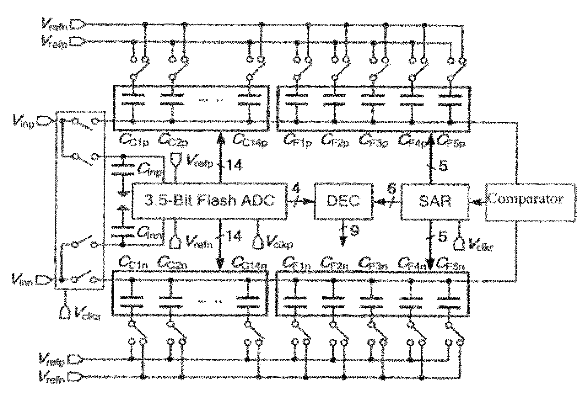
"The present invention provides a subrange analog-to-digital converter (ADC) with improved differential non-linearity (DNL) and sampling speed. The subrange ADC includes a X.5-bit flash ADC, a Y-bit SAR ADC, and a (X+Y)-bit segmented capacitive digital-to-analog converter (DAC). The flash ADC controls thermometer coarse capacitors of the DAC and the SAR ADC controls binary fine capacitors. Compared with a pure binary DAC, the flash ADC improves DNL. The sampling speed of the subrange ADC as a whole is also raised due to the simultaneous engagement of the analog-to-digital conversions of the X bits. The subrange ADC has a positive and a negative input terminals, a first capacitor array with 2(2(N+1)−2) capacitors, each of which has a first and a second terminals, divided into N groups, where each group represents N bits, and a reference voltage generating circuit formed by 2(N+1)−2 resistors. The method for adjusting the subrange ADC involves comparing the positive and negative voltage values generated via the input signal with two sets of divided voltages to generate two sets of output signals, and determining simultaneously whether to adjust the voltage value of each bit of the N groups according to the two sets of output signals."

Problems solved by technology

Also, complex switching network results in high technical difficulty in designing high-speed and high-resolution subrange ADCs.
Besides, a SAR ADC could achieve a high energy efficiency of analog-digital conversion, but the SAR ADC has to go through many cycles to finish a data conversion, and thus the operation speed is limited.
However, the resistance value of the resistor ladder in the flash ADC is not allowed to be too small for the reason of low power consumption.
But a drawback of the binary weighted capacitor array is that the capacitance value of its maximum bit is a sum of all the remaining bits.
When a high resolution version is designed, an overly large input capacitance value will limit the input bandwidth and result in that the capacitor switching requires even larger energy consumption.
During the whole conversion procedure, the capacitor having the maximum weight in the capacitor array (being one half of the whole capacitance value in the capacitor array) requires the longest settling time, and it is the main bottleneck of the operational speed of the SAR ADC.

Method used


Image

  • Subrange analog-to-digital converter and method thereof
  • Subrange analog-to-digital converter and method thereof
  • Subrange analog-to-digital converter and method thereof

Examples


embodiment 1

[0042]2. A converter further comprising a first and a second bootstrapped switches, an error correction circuit and a comparator electrically connected to the positive and the negative terminals, wherein the positive and the negative input terminals receive an input signal, the input signal is a differential signal, the first and the second bootstrapped switches are respectively connected between the positive input terminal and the comparator, and between the negative input terminal and the comparator for completely passing the differential signal through the positive and the negative input terminals, the SAR ADC includes a first digital control circuit, the flash ADC includes a second digital control circuit, and the error correction circuit electrically connects with the SAR ADC and the flash ADC and generates a digital code matched to the input signal.

[0043]3. A converter according to Embodiment 1 or 2, wherein the second capacitor array is configured to be one of the remaining ...

embodiment 6

[0050]7. A converter , wherein the 2(2(N+1)−2) capacitors are equivalent capacitors, in which each the first terminal of a first set of the 2(2(N+1)−2) capacitors is electrically connected to the positive input terminal, each the first terminal of the other set of the 2(2(N+1)−2) capacitors is electrically connected to the negative input terminal and each of the first set and the other set of the 2(2(N+1)−2) capacitors has (2(N+1)−2) capacitors.

[0051]8. A converter according to Embodiment 6 or 7 further comprising a successive approximation ADC (SAR ADC) including a second capacitor array having a plurality of bits and at least one of the capacitors with a first and a second terminals, wherein each the bit of the first and the second capacitor arrays electrically connects with at least one the capacitors, the first terminal electrically connects with one of the positive and negative input terminals, and the second terminal switchably connects with a first and a second reference volt...

embodiment 12

[0059]13. A method , wherein each of the two sets of divided voltages has (2(N+1)−2) voltages and each of the two sets of output signals has (2(N+1)−2) output signals.

[0060]14. A method according to Embodiment 12 or 13 further comprising a step of generating N digital codes respectively corresponding to the N bits according to the voltage value of each the capacitor representative of each the bit of the N groups after an adjustment in the determining step is finished.

[0061]15. A method according to anyone of the above-mentioned Embodiments, wherein the subrange ADC has M bits counted from a most significant bit (MSB) to a least significant bit (LSB), further comprising steps of:

[0062]providing a capacitor array having at least one capacitor with a first and a second terminals and configured to be one of the remaining (M−N) bits and the remaining (M−N−1) bits of the M bits, wherein each the bit electrically connects with the at least one capacitor, the first terminal receives the inp...


PUM


Abstract

The configurations and adjusting method of a subrange analog-to-digital converter (ADC) are provided. The provided subrange ADC includes a X.5-bit flash ADC, a Y-bit SAR ADC and a (X+Y)-bit segmented capacitive digital-to-analog converter (DAC).

Description

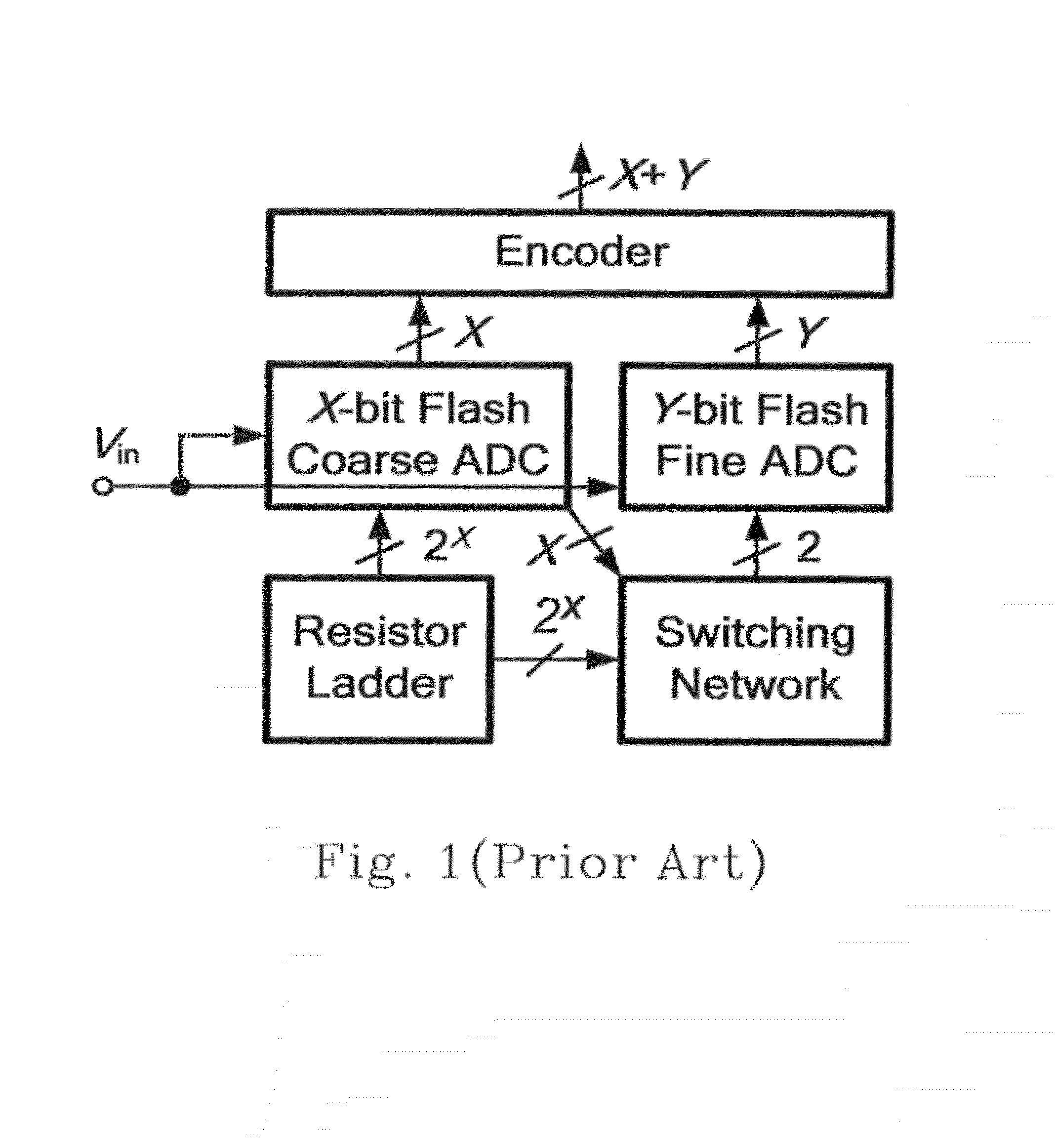
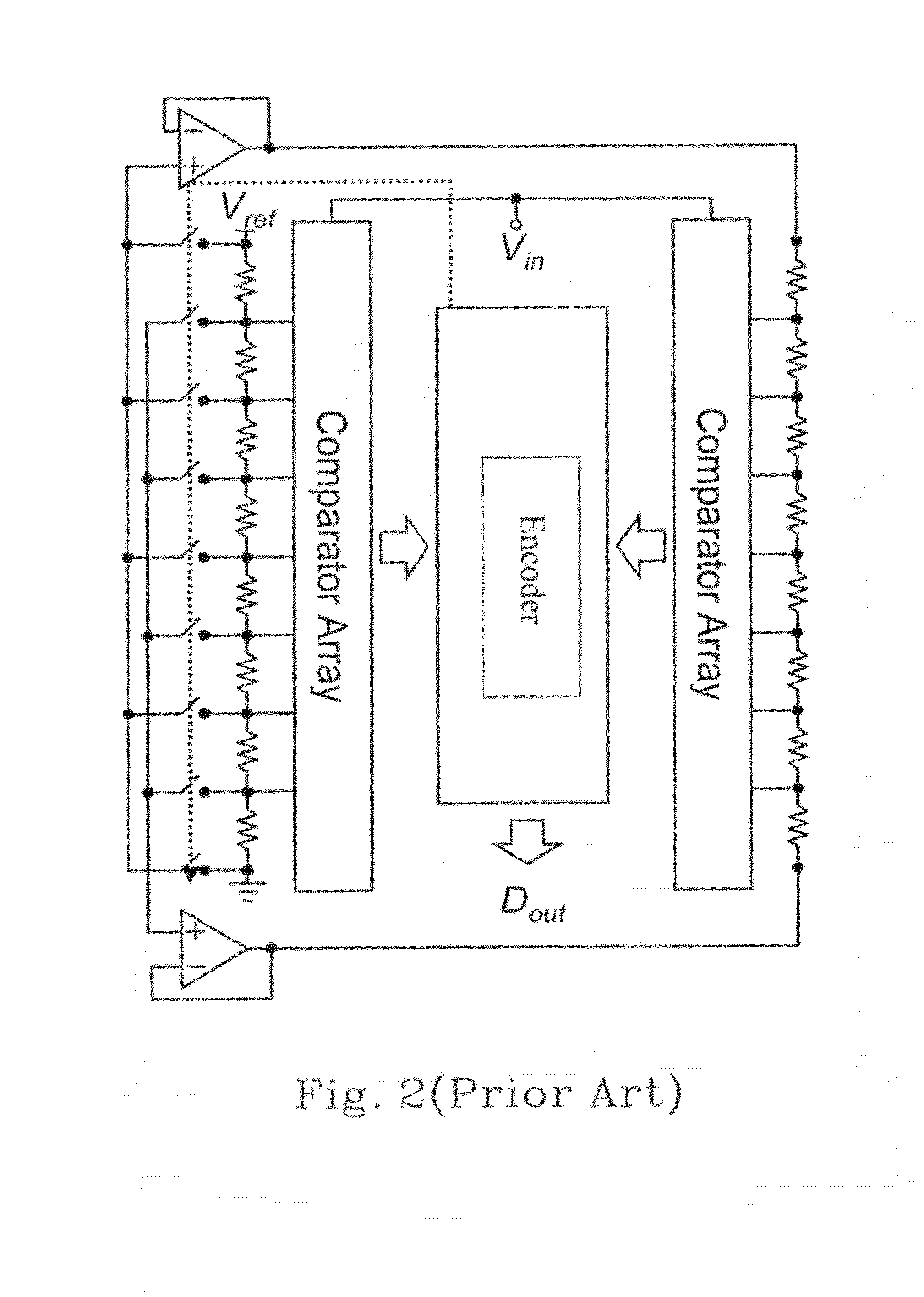
FIELD OF THE INVENTION[0001]The application claims the benefit of Taiwan Patent Application No. 099144332, filed on Dec. 16, 2010, in the Taiwan Intellectual Property Office, the disclosures of which are incorporated herein in their entirety by reference.[0002]The present invention relates to a subrange analog-to-digital converter (ADC). More particularly, it relates to a subrange ADC including a X.5-bit flash ADC, a Y-bit successive approximation analog-to-digital converter (SAR ADC) and a (X+Y)-bit segmented capacitive digital-to-analog converter (DAC).BACKGROUND OF THE INVENTION[0003]Conventionally, the subrange ADC includes two flash ADCs. FIG. 1 shows a schematic diagram of a conventional subrange ADC. In FIG. 1, the subrange ADC receives an input voltage Vin and includes a X-bit flash coarse ADC, a resistor ladder, a Y-bit flash fine ADC, a switching network and an encoder for generating a digital code having (X+Y) bits corresponding to an input voltage Vin. FIG. 2 is a 6-bit ...

Claims


Application Information

Patent Timeline
Patent Type & Authority Patents(United States)
IPC IPC(8): H03M1/12
CPCH03M1/145H03M1/468H03M1/466H03M1/365
Inventor CHANG, SOON-JYHLIN, YING-ZULIU, CHUN-CHENG
Owner NAT CHENG KUNG UNIV
Learn More