Compact loaded-waveguide element for dual-band phased arrays

a phased array and loaded technology, applied in waveguides, waveguide type devices, one-port networks, etc., can solve the problems of not meeting the design attempt of dual-band phased arrays has not been found to meet all of the necessary requirements for some applications, and the limitations of high-band performan

Active Publication Date: 2012-07-10
RAYTHEON CO
View PDF24 Cites 0 Cited by
  • Summary
  • Abstract
  • Description
  • Claims
  • Application Information

AI Technical Summary

Benefits of technology

[0013]It would be advantageous to be able to integrate low-band sensors into a high-band array so that all high and low-band elements share the same aperture while both bands could be scanned to wide angles. Such a dual-band system could provide greater flexibility for multi-function missions, reduce aperture area, and may allow re-use of back-end electronics. To achieve this integration, the low-band element preferably should be very compact to minimize interference to high-band performance. The low-band element also needs to have the desired wide scan angle performance over a broad bandwidth. No such an element is known to exist that meets these difficult requirements.
[0028]In one embodiment, at least one of the high-band radiating array and the low-band radiating array has a size and spacing enabling the antenna to be operable to scan at scan angles greater than or equal to sixty degrees from boresight with a bandwidth greater than or equal to 15%.
[0030]The first opening is sized to receive the coaxial conductor. The second opening is formed in an orientation that is substantially perpendicular to the first opening, the second opening being formed in a first portion of the dielectric section, wherein the second opening is substantially hollow and has a lining comprising an electrically conductive material that is operably coupled to the coaxial conductor disposed in the first opening. The plurality of step transitions are disposed after the first portion of the dielectric section, the plurality of step transitions cooperating to provide impedance matching and reduce the height of the respective antenna element from a first height at the input to the antenna element to a second height at the output of the antenna element, wherein at least one of the step transitions is adapted to be disposed within the waveguide and to be operably coupled between the dielectric section and a planar section, wherein the at least one step transition partially fills an interior first portion of the waveguide at the first end, wherein at least a second portion of the waveguide adjacent to the first portion is filled with air, and wherein the size of the step transition that partially fills the waveguide is selected at least in part to provide impedance matching between the dielectric section and the waveguide.
[0036]The first opening is sized to receive the coaxial conductor. The second opening is formed in an orientation that is substantially perpendicular to the first opening, the second opening being formed in a first portion of the dielectric section, wherein the second opening is substantially hollow and has a lining comprising an electrically conductive material that is operably coupled to the coaxial conductor disposed in the first opening. The plurality of step transitions is disposed after the first portion of the dielectric section, the plurality of step transitions cooperating to provide impedance matching and reduce the height of coaxial to waveguide transition from a first height at the first end to a second height at the second end, wherein at least one of the step transitions is adapted to be disposed within and to partially fill a waveguide operably coupled to the dielectric section, wherein the size of the step transition that partially fills the waveguide is selected at least in part to provide impedance matching between the dielectric section and the waveguide.

Problems solved by technology

No such an element is known to exist that meets these difficult requirements.
Previous design attempts for dual-band phased arrays have not been found to meet all of the necessary requirements for some applications.
However, for this design, like many others, there are limitations of high-band performance, because at high-band, the scan performance will be limited due to grating lobes.
However, it is possible that the dipoles can cause blockage to X-band, resulting in severe (and undesirable) interaction between L and X bands.

Method used


Image

  • Compact loaded-waveguide element for dual-band phased arrays
  • Compact loaded-waveguide element for dual-band phased arrays
  • Compact loaded-waveguide element for dual-band phased arrays

Examples


Embodiment Construction

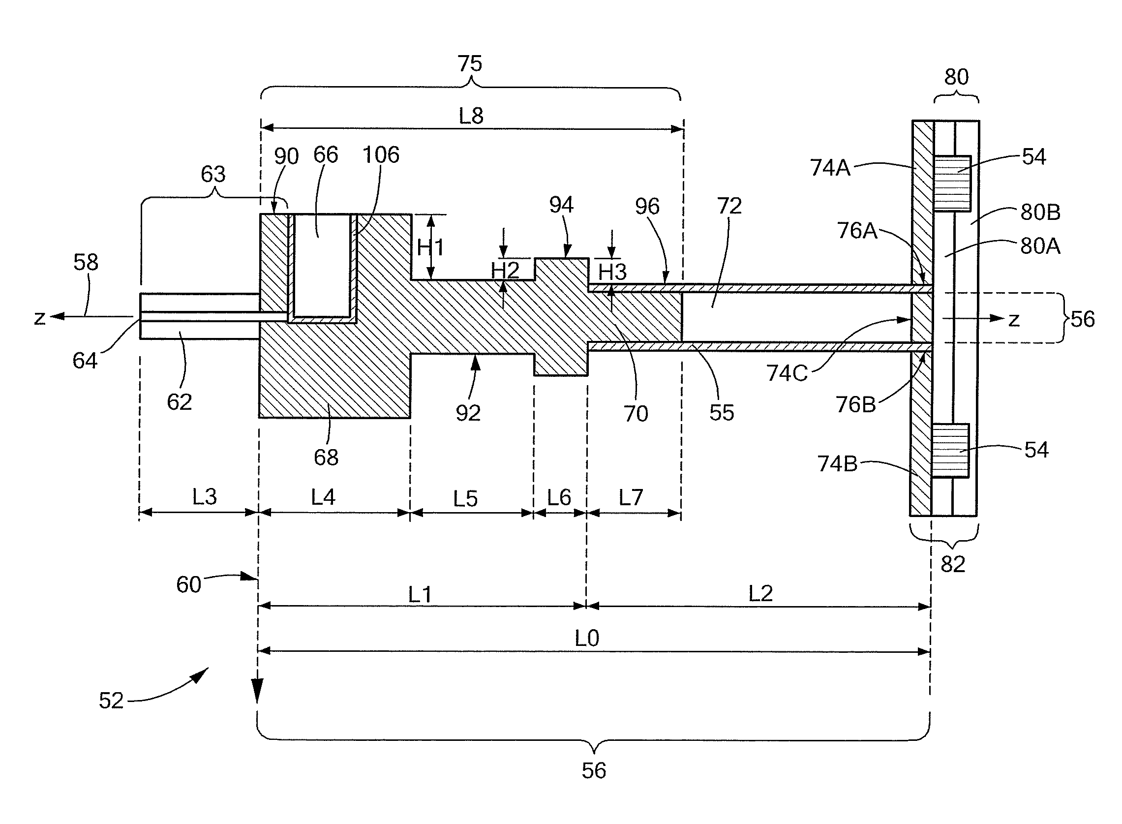
[0051]In the following description, many dimensions, relative dimensions, etc., are expressed in terms of wavelengths, such as where λ0 (or, as applicable, λL for the low-band or λH for the high-band) is used to indicate the wavelength at the middle of the operating frequency band. As those of skill in the art are aware, the wavelength is dependent on the antenna frequency and / or frequency band in question. It is intended that the dimensions and relative dimensions given herein are applicable over a number of bands and wavelengths, and it is not intended for the invention to be limited to any particular wavelengths. For example, the embodiments of the invention can be constructed for virtually any required frequency, by scaling the size of the device based on the wavelength that corresponds to the frequency being used. Thus, if an embodiment lists an overall device length, for example, of one wavelength (λ), a first further embodiment for a device at a first frequency may be about t...


PUM


Abstract

An array antenna is provided that operates at high-band and low-band, comprising a first array of high-band radiators and a second array of low-band radiators, each respective low-band radiator disposed so as to be interleaved between the high-band radiators so as to share an aperture with the high-band radiators. Each low-band radiator comprises a coaxial section, a dielectric section, a waveguide, and a planar section. The dielectric section is formed of a continuous piece of dielectric material and includes a hollow opening formed perpendicular to the coaxial section, and a plurality of step transitions, wherein at least one of the step transitions is disposed within and partially fills the waveguide operably coupled to the planar section. The planar section is oriented to the portion of high-band radiators such that the output of the respective low-band radiator is disposed between and within the spacing between adjacent high-band-radiators.

Description

FIELD OF THE INVENTION[0001]Embodiments of the invention generally relate to devices, systems, and methods for providing antenna elements. More particularly, the invention relates to devices, systems and methods for structures and devices providing a compact and simple to manufacture element for dual-band phased array antennas.BACKGROUND[0002]Modern commercial and military systems such as radar systems, and satellite communication systems, often perform multiple functions that can require a plurality of different radar beams at different wavelengths. Examples of these functions include surveillance of targets and objects at various ranges / distances, air traffic control, navigation, weapons control, weather surveillance, satellite uplink and downlink signaling, telecommunications, and Internet communications. In many of the environments in which such systems are deployed, it can be difficult to provide multiple antennas to support the multiple different beams because of space and / or ...

Claims


Application Information

Patent Timeline
Patent Type & Authority Patents(United States)
IPC IPC(8): H01Q1/50H03H7/38H01P1/00H01P3/06H01Q21/00
CPCH01Q21/064H01Q5/42H01Q21/065
Inventor CHANG, YUEH-CHIKOMISAREK, KENNETH S.FAGERLUND, GREGORY M.ROWLAND, LANDON L.CHANG, KAICHIANGCAPLAN, BENJAMIN L.
Owner RAYTHEON CO
Why Eureka
Try Eureka