Self-calibration method of a reading circuit of a nonvolatile memory

a nonvolatile memory and reading circuit technology, applied in the field of circuit self-calibration method, can solve the problems of increasing the chip increasing the test cost, increasing the investment of test equipment and test cost, etc., and achieves the effect of improving the reliability of the memory without increasing the circuit area and the test cos

Active Publication Date: 2012-05-22
SHANGHAI HUAHONG GRACE SEMICON MFG CORP
View PDF3 Cites 4 Cited by
  • Summary
  • Abstract
  • Description
  • Claims
  • Application Information

AI Technical Summary

Benefits of technology

[0020]The present invention, not requiring an additional fuse or difference unit, can solve a deadlock problem securely and reliably without increasing circuit area and test cost, and be widely applied to OTP, MTP and EEPROM of various processes or various nonvolatile memories such as Flash EEPROM, improving reliability of the memory effectively.

Problems solved by technology

This set requires storing N-bit data into a special cell of the memory, whereas the set datum needs to be retrieved when the set is read, thus resulting in deadlock.
1. A polycrystalline fuse is adopted, as shown in FIG. 1. Number of PAD will be increased by this solution, thus increasing area of the chip and the test cost as well.
2. Laser calibration is usually adopted in a dynamic random access memory (DRAM) and a product of an owner chip factory (IDM). For a universal product of an agent factory (Foundry), this method is seldom adopted due to significant increase of test equipment investment and test cost.
3. A differential nonvolatile memory is adopted, as shown in FIG. 2, such as a nonvolatile static random access memory (nonvolatile SRAM). That is, a new circuit module outside and independent of the nonvolatile memory module stores each data bit using two physical cells based on the differential principle, with the storage results contrary to each other. The additional storage module that this solution introduces will increase the chip area, and an additional test on this module is required during test of a silicon chip as well, thus increasing the test cost.

Method used


Image

  • Self-calibration method of a reading circuit of a nonvolatile memory
  • Self-calibration method of a reading circuit of a nonvolatile memory
  • Self-calibration method of a reading circuit of a nonvolatile memory

Examples


Embodiment Construction

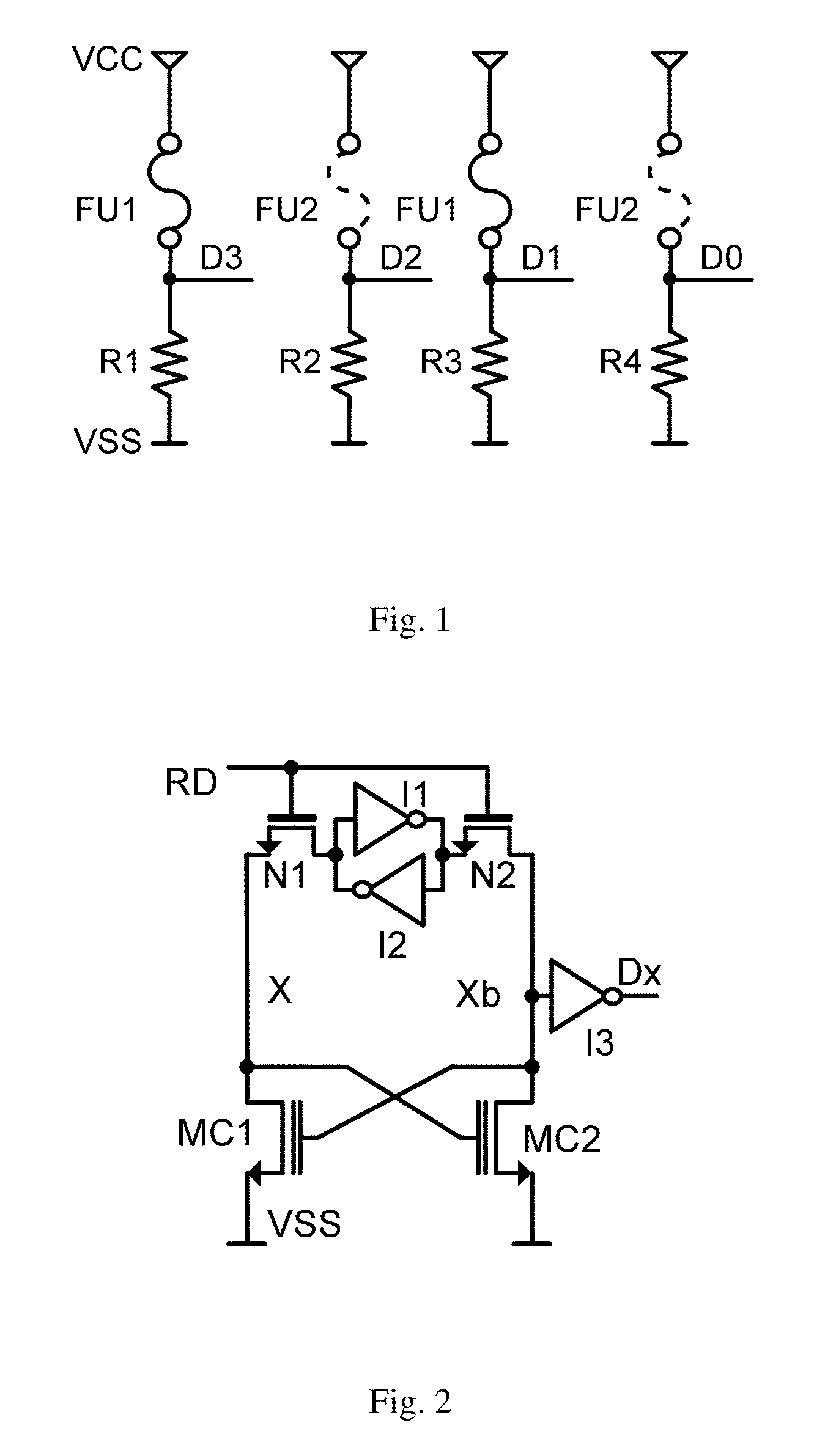
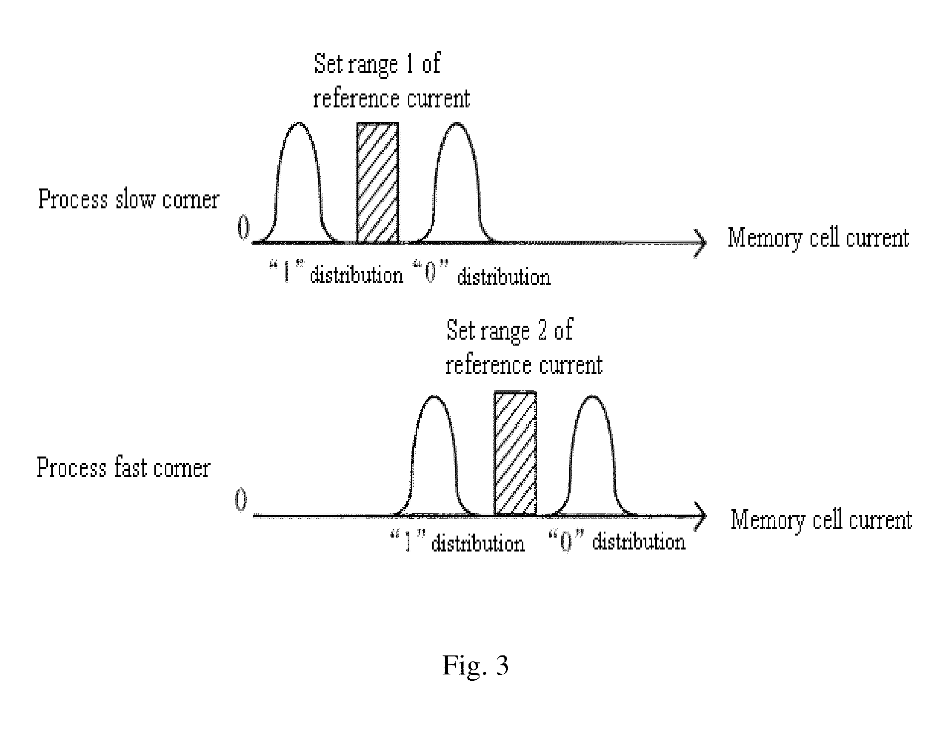
[0029]The present invention discloses a selfcalibration method of a reading circuit of a nonvolatile memory, by which binary trimming data are stored in a bit-pair form into the memory during a product test, a value of the trimming data having recorded a value of a reference current required by the memory for normal work, the bit-pair form meaning that each digit of the trimming data is represented by 2-digit different binary numbers “0” and “1” with a changed order; after the memory circuit is powered on, a sense amplifier controlling the value of the reference current is regulated, and when “0” and “1” in the outputted trimming data stored in the bit-pair form have the same quantities, the trimming data are read, thus obtaining the value of the reference current, according to which the outputted reference current of the sense amplifier is controlled.

[0030]In an embodiment of the above technical solution, “0” is represented by a 2-digit binary number “01”, and “1” by a 2-digit bina...


PUM


Abstract

A self-calibration circuit of a nonvolatile memory includes a trimming data storage module, a sense amplifier module, a logic judgment module, and a scanning module. The nonvolatile memory circuit includes a memory cell array and the self-calibration circuit of the reading circuit of the nonvolatile memory. Without requiring an additional fuse or differential unit, the self-calibration circuit of a nonvolatile memory solves a deadlock problem securely and reliably without increasing circuit area and test cost, and be widely applied to OTP, MTP and EEPROM of various processes or various nonvolatile memories such as Flash EEPROM, MRAM, and FeRAM.

Description

TECHNICAL FIELD[0001]The present invention relates to a circuit selfcalibration method, particularly to a selfcalibration method of a reading circuit of a nonvolatile memory. The present invention further relates to a calibration circuit, particularly to a selfcalibration circuit of the reading circuit of the nonvolatile memory. The present invention furthermore relates to a nonvolatile memory circuit.BACKGROUND TECHNOLOGY[0002]For a nonvolatile memory cell of advanced processes such as Flash EEPROM, due to decreasing dimensions, current of the Cell will change greatly under various process deviation corner. If “1” is defined as a small current and “0” a great current, it is possible that the current of Cell “1” in a fast corner is greater than that of Cell “0” in a slow corner. In order to achieve high reliability, it is required that a trimming datum is set for a reference current of the sense amplifier for different chips. This set requires storing N-bit data into a special cell ...

Claims


Application Information

Patent Timeline
Patent Type & Authority Patents(United States)
IPC IPC(8): G11C7/00
CPCG11C7/08G11C7/1045G11C16/28G11C29/02G11C29/026G11C29/028G11C2029/5006G11C2207/2254
Inventor WANG, NANYAO, XIANG
Owner SHANGHAI HUAHONG GRACE SEMICON MFG CORP
Why Eureka
Try Eureka