Magnetic reading head and magnetic recording apparatus
a reading head and magnetic recording technology, applied in the manufacture of flux-sensitive heads, instruments, record information storage, etc., can solve the problems of unstable magnetic material magnetization in each of the existing cpp-gmr heads and tmr heads, difficult to maintain magnetization, and increase magnetic noise, so as to reduce the volume of a free layer, suppress the increase of magnetic noise, and reduce electrical noise
- Summary
- Abstract
- Description
- Claims
- Application Information
AI Technical Summary
Benefits of technology
Problems solved by technology
Method used
Image
Examples
example 1
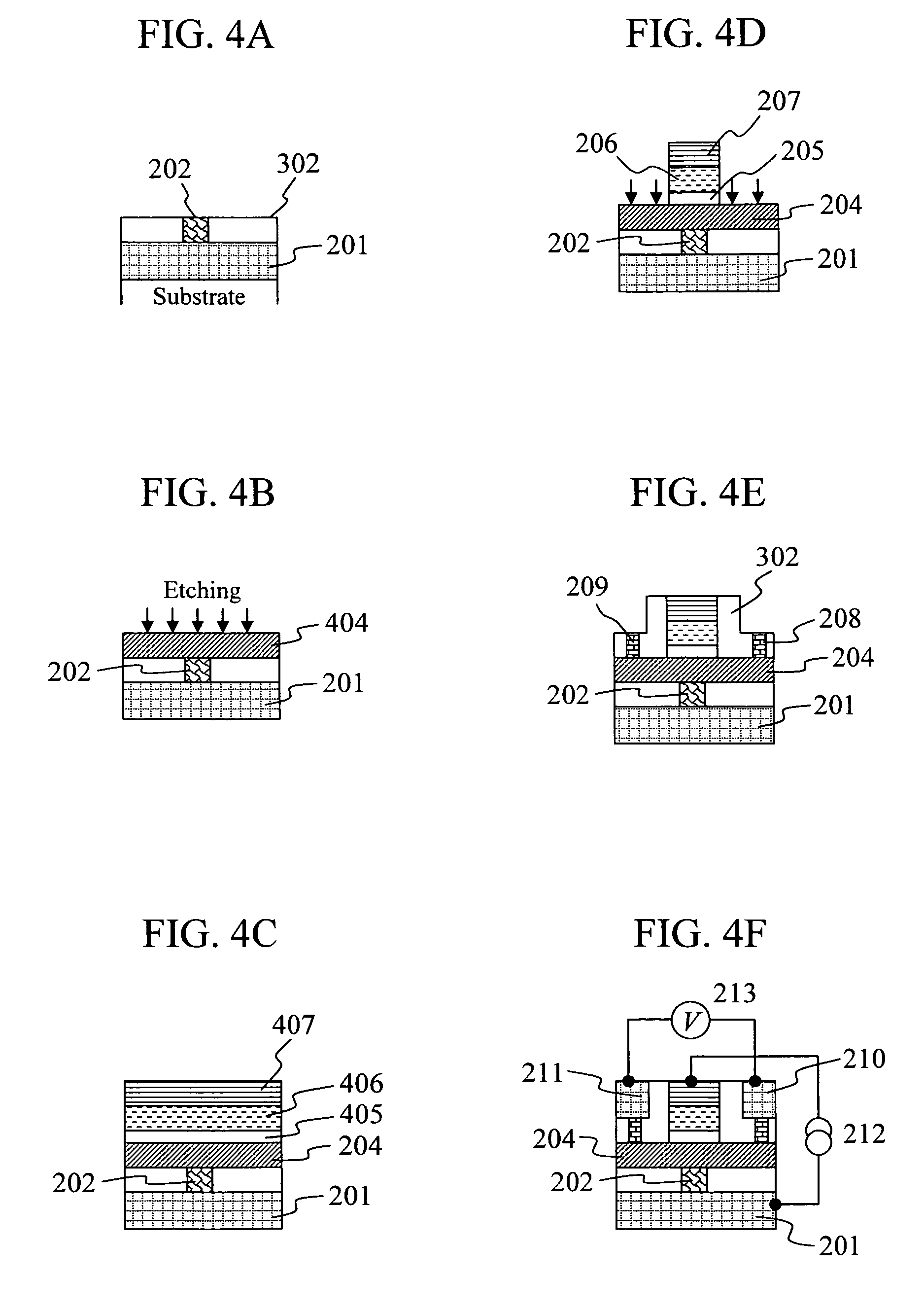
[0060]A magnetic reading head including the second modulated spin accumulation device by magnetic field as shown in FIG. 2 was manufactured through the steps shown in FIGS. 4A to 4F. As a substrate, prepared was a commonly-used substrate on which a shield layer was formed. The commonly-used substrate was a SiO2 substrate or a glass substrate (or was a magnesium oxide substrate, a GaAs substrate, an AlTiC substrate, a SiC substrate, an Al2O3 substrate or the like, instead). The shield layer was formed with a film forming apparatus using an RF sputtering method, a DC sputtering method, a molecular beam epitaxy method (MBE) or the like. For example, in the case where an RF sputtering method is employed for forming the shield layer, a predetermined film is caused to grow in an Ar atmosphere under conditions where a pressure is on the order of 0.1 to 0.001 Pa, and a power is 100 W to 500 W. As a substrate on which the device was to be formed, used was either one of the above substrates w...
example 2
[0068]A magnetic reading head including the third modulated spin accumulation device by magnetic field (refer to FIG. 5) according to the present invention was manufactured through the steps shown in FIGS. 8A to 8F. The following steps 1 to 6 correspond to FIGS. 8A to 8F, respectively.
Step 1: Forming a Pinned Layer (Magnetic Material)
[0069]As an electrode, a Pt film was formed in a thickness of 100 nm on a Si substrate of 3 inches provided with a thermal oxide film using an RF magnetron sputtering apparatus. On the Pt electrode, a MnIr film with a thickness of 10 nm to serve as an antiferro magnetic material, a CoFeB film with a thickness of 4 nm to serve as a pinned layer were sequentially formed. Then, an MgO film with a thickness of 2 nm to serve as a barrier layer was formed on the CoFeB film. Thereafter, as a pattern for the pinned layer, a square pattern of 1×1 μm2 was transferred onto the barrier layer with an I-line stepper, and the thus-formed layers were patterned by ion m...
PUM
| Property | Measurement | Unit |
|---|---|---|
| gap width | aaaaa | aaaaa |
| total thickness | aaaaa | aaaaa |
| pressure | aaaaa | aaaaa |
Abstract
Description
Claims
Application Information
 - R&D
- Intellectual Property
- Life Sciences
- Materials
- Tech Scout
- Unparalleled Data Quality
- Higher Quality Content
- 60% Fewer Hallucinations
Browse by: Latest US Patents, China's latest patents, Technical Efficacy Thesaurus, Application Domain, Technology Topic, Popular Technical Reports.
© 2025 PatSnap. All rights reserved.Legal|Privacy policy|Modern Slavery Act Transparency Statement|Sitemap|About US| Contact US: help@patsnap.com


