Semiconductor device
a technology of semiconductors and circuits, applied in the field of semiconductor devices, can solve the problems of large time and cost for tuning, and complicated control of tuning circuits, so as to reduce detection temperature, prevent cost increase, and increase the size of tuning circuits
- Summary
- Abstract
- Description
- Claims
- Application Information
AI Technical Summary
Benefits of technology
Problems solved by technology
Method used
Image
Examples
first embodiment
[0067]Next, the configuration and operation of a temperature detection circuit according to the first embodiment of the invention will be described with reference to FIGS. 8 to 12.
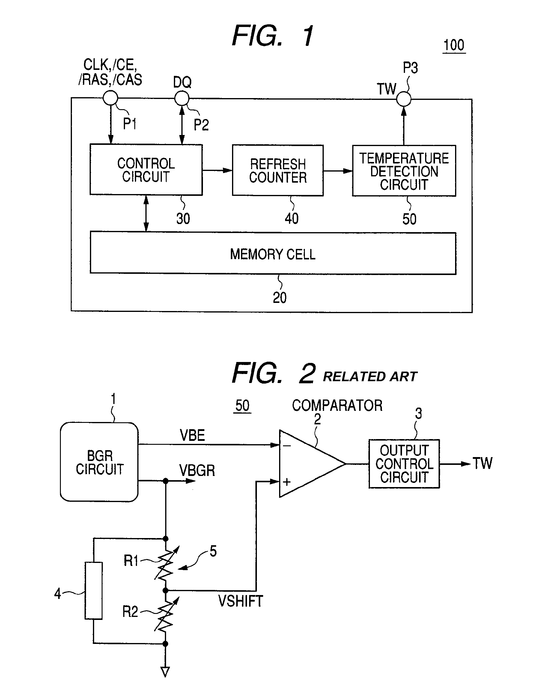
[0068]FIG. 8 is a block diagram showing the configuration of a temperature detection circuit 50A according to the first embodiment. The same configurations as in the temperature detection circuit 50 described with reference to FIG. 2 are denoted by the same reference numerals, and their description will not be repeated.
[0069]Further, the temperature detection circuit 50A can be substituted for the temperature detection circuit 50 of the memory chip 100 shown in FIG. 1. The temperature detection circuit 50A shown in FIG. 8 has, in addition to the variable resistors R1 and R2 configuring the level shift circuit 5, an additional resistor RU (a first resistor) coupled between the output node of the VBGR voltage of the BGR circuit 1 and the variable resistor R1 and an additional resistor RD (a second resistor) ...
second embodiment
[0090]Next, the configuration and operation of a temperature detection circuit according to the second embodiment of the invention will be described with reference to FIGS. 13 to 16.
[0091]FIG. 13 is a block diagram showing the configuration of a temperature detection circuit 50B according to the second embodiment. The same configurations as in the temperature detection circuit 50A described with reference to FIG. 8 are denoted by the same reference numerals, and their description will not be repeated.
[0092]In the temperature detection circuit 50B shown in FIG. 13, a comparator 2A has a hysteresis characteristic in the normal mode and does not have a hysteresis characteristic in the test mode.
[0093]FIG. 14 shows that the VSHIFT voltage is increased in the test mode so that the point of intersection of the VSHIFT voltage and the VBE voltage, that is, the detection temperature changes to 85° C. In FIG. 14, the horizontal axis indicates the temperature (° C.), and the vertical axis indi...
third embodiment
[0100]Next, the configuration and operation of a temperature detection circuit according to the third embodiment of the invention will be described with reference to FIGS. 17 to 21.
[0101]FIG. 17 is a block diagram showing the configuration of a temperature detection circuit 50C according to the third embodiment. The same configurations as in the temperature detection circuit 50A described with reference to FIG. 8 are denoted by the same reference numerals, and their description will not be repeated.
[0102]In the temperature detection circuit 50 shown in FIG. 2 and the temperature detection circuit 50A shown in FIG. 8, the determination result of the chip inside temperature is not outputted in real time in the normal mode, but the output control circuit 3 updates the determination result at predetermined intervals in synchronization with rising edges of an upper counter of the refresh counter 40 in the memory chip 100 (FIG. 1) and outputs it to the outside.
[0103]On the other hand, an ...
PUM
| Property | Measurement | Unit |
|---|---|---|
| temperature | aaaaa | aaaaa |
| temperature | aaaaa | aaaaa |
| temperature | aaaaa | aaaaa |
Abstract
Description
Claims
Application Information
 - R&D
- Intellectual Property
- Life Sciences
- Materials
- Tech Scout
- Unparalleled Data Quality
- Higher Quality Content
- 60% Fewer Hallucinations
Browse by: Latest US Patents, China's latest patents, Technical Efficacy Thesaurus, Application Domain, Technology Topic, Popular Technical Reports.
© 2025 PatSnap. All rights reserved.Legal|Privacy policy|Modern Slavery Act Transparency Statement|Sitemap|About US| Contact US: help@patsnap.com


