
Semiconductor integrated circuit device having fail-safe mode and memory control method

a technology of integrated circuit device and memory control, which is applied in the direction of instruments, coding, code conversion, etc., can solve the problems of not being able to cure the defect by replacing the block, and the defect is a defect on all blocks, so as to achieve the effect of reliable operation

Active Publication Date: 2011-11-08
RENESAS ELECTRONICS CORP
View PDF25 Cites 35 Cited by
  • Summary
  • Abstract
  • Description
  • Claims
  • Application Information

AI Technical Summary

Benefits of technology

This patent describes a semiconductor integrated circuit device and memory control method that can continue operating even if there is a defect in the flash memory. The device includes a flash memory and flash control unit, as well as a processor. The processor commands the flash control unit to perform various operations, such as reading and writing data on the flash memory. The device has a normal mode and a fail-safe mode for error correction. In the normal mode, all further usage of the flash memory is stopped if a defect is detected in the verify operation after writing data. In the fail-safe mode, errors are corrected and the flash memory can continue to be used even if a defect is detected. The memory control program includes a normal mode operation sequence and a fail-safe mode operation sequence. The invention allows for reliable operation and limited functions even if a defect occurs in the flash memory.

Problems solved by technology

In the case of a flash memory, the bit lines are often jointly shared by all blocks so if a defect such as a locked state occurs on a specific bit line then that defect is a defect on all blocks.
If a breakdown occurs on the word lines / bit lines of the memory cell, then that affects the entire memory so merely replacing the block will not cure the defect.

Method used


Image

  • Semiconductor integrated circuit device having fail-safe mode and memory control method
  • Semiconductor integrated circuit device having fail-safe mode and memory control method
  • Semiconductor integrated circuit device having fail-safe mode and memory control method

Examples


Embodiment Construction

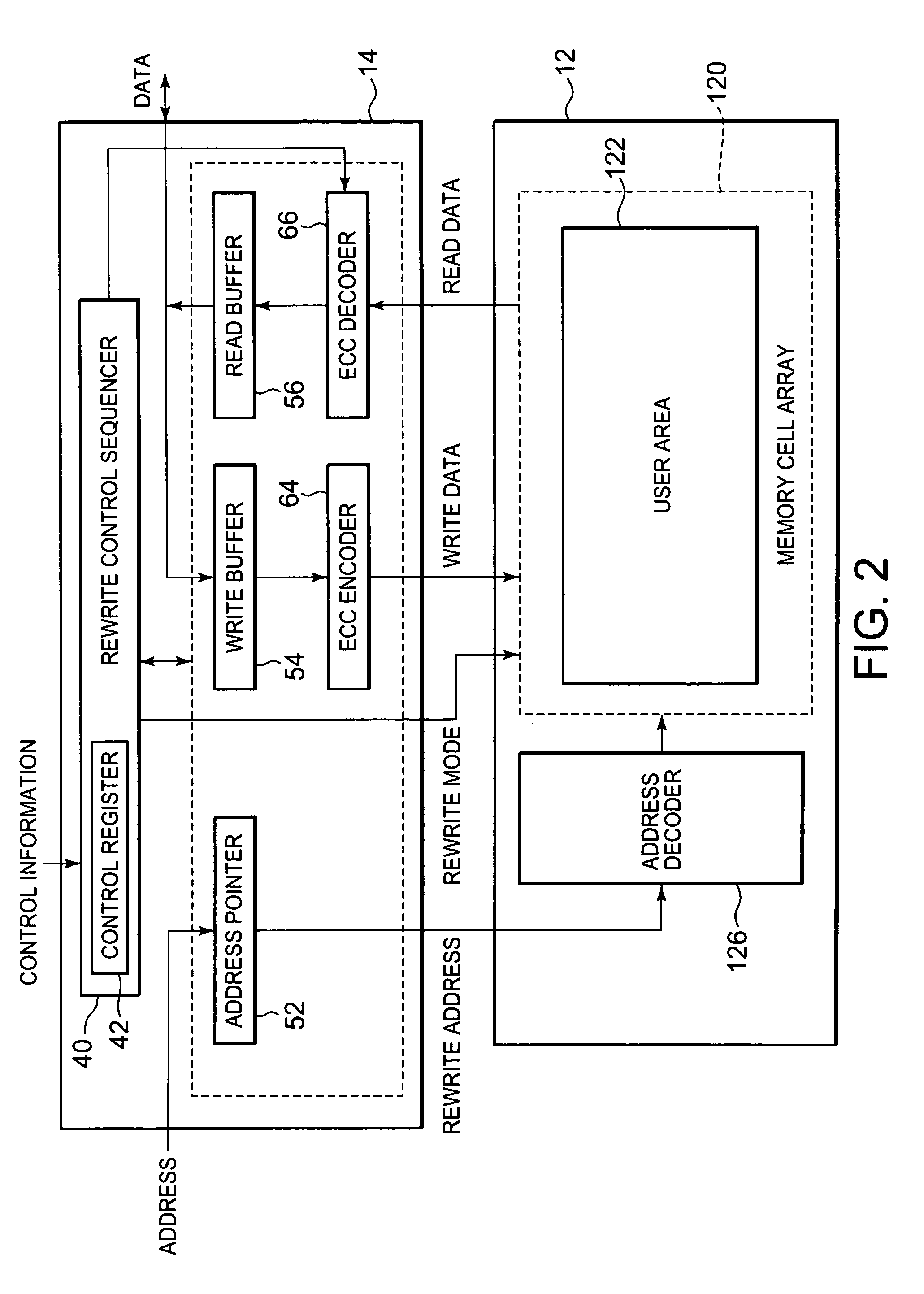
[0033]FIG. 1 shows the structure of the microprocessor of an exemplary embodiment of this invention. The microprocessor contains a CPU (central processing unit) 20, a RAM (random access memory) 30, and a flash unit 10. The CPU 20 loads (read out) commands from the flash unit 10 by way of the bus 24, loads data for storage onto the RAM 30 and writes data such as processed data into the RAM 30 via the bus 22. Data that must be retained even if the power is not supplied is stored in the flash unit 10. This data is loaded and processed. The flash unit 10 contains a flash memory 12 for retaining data and a flash control unit 14 for controlling the reading and controlling the writing of the flash memory 12. Data stored in the flash unit 10 can be written and read out by way of the peripheral bus 26.

[0034]FIG. 2 shows the structure of the flash unit 10 of the first embodiment of this invention. This figure shows the memory control method implemented by software in the first embodiment. The...


PUM


Abstract

An integrated circuit device contains a flash memory, a flash control unit for controlling the rewriting and reading on the flash memory, and a processor unit. The processor unit includes a normal mode and a fail-safe mode as the operating states. In normal mode, when a defect is detected during the verify operation after writing data onto the flash memory then any further use of the flash memory is stopped. In fail-safe-mode, when a defect is detected during the verify operation after writing data onto the flash memory, the error is corrected and flash memory usage continues. The operating state is normal mode, and when the verify operation detects a defect after normal mode erase operation, the operation shifts to fail-safe mode.

Description

BACKGROUND OF THE INVENTION[0001]1. Field of the Invention[0002]This invention relates to a semiconductor integrated circuit device for storing a flash memory and also relates to a memory control method for regulating access to that flash memory.[0003]2. Description of Related Art[0004]Demand has been increasing in recent years for EEPROM emulations to add a small data capacity to the flash memory as a substitute for an external EEPROM. These EEPROM applications require an extremely large number of rewrite operations and so must provide reliability for this (large) number of rewrites.[0005]In the technology disclosed in Japanese Patent Laid Open Application No. 2006-48893, the hardware selects a spare block address as the physical address from the defect block mapping information and the control address that was received. The flash memory includes a memory cell array unit, a defect block mapping register unit, an address selector unit, and a defect block status control unit. The mem...

Claims


Application Information

Patent Timeline
Patent Type & Authority Patents(United States)
IPC IPC(8): G11C29/00G11C11/34H03M13/00
CPCG06F11/1068G06F11/0796G06F11/141G11C2029/0409
Inventor KONDO, TAKAO
Owner RENESAS ELECTRONICS CORP
Learn More