Semiconductor device
a semiconductor device and semiconductor technology, applied in the direction of semiconductor devices, basic electric elements, electrical equipment, etc., can solve the problems of difficult to achieve ideal transconductance characteristics, field-effect semiconductor devices tend to be noisy, and noise between adjacent lines, so as to improve distortion characteristics
- Summary
- Abstract
- Description
- Claims
- Application Information
AI Technical Summary
Benefits of technology
Problems solved by technology
Method used
Image
Examples
first embodiment
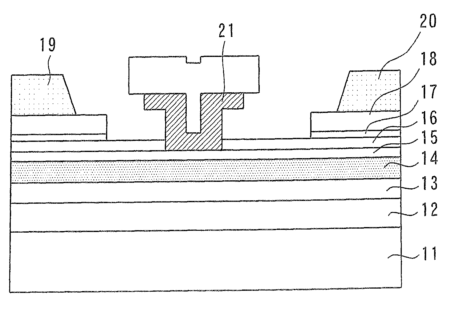
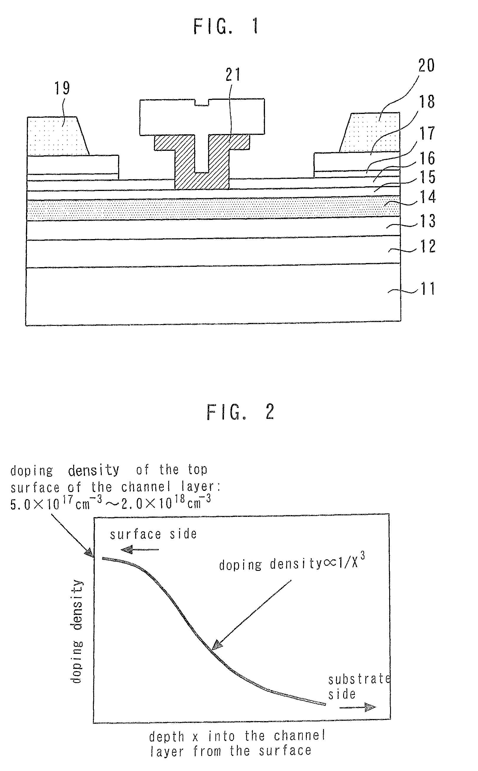
[0032]FIG. 1 is a cross-sectional view of a semiconductor device according to a first embodiment of the present invention. Referring to FIG. 1, the following layers are sequentially formed on top of one another on a semi-insulating GaAs substrate 11 (referred to as a “compound semiconductor substrate” in the appended claims): an undoped AlGaAs / undoped GaAs superlattice buffer layer 12; an undoped GaAs buffer layer 13 (referred to simply as a “buffer layer” in the appended claims); an n-type GaAs channel layer 14 (referred to simply as a “channel layer” in the appended claims); an n-type AlGaAs Schottky junction forming layer 15 (referred to simply as a “Schottky junction forming layer” in the appended claims); an n-type GaAs lower contact layer 16, an n-type AlGaAs etch stopper layer 17; and an n+-type GaAs upper contact layer 18.
[0033]A source electrode 19 and a drain electrode 20 are formed on the n+-type GaAs upper contact layer 18 (i.e., above the n-type AlGaAs Schottky junction...
second embodiment
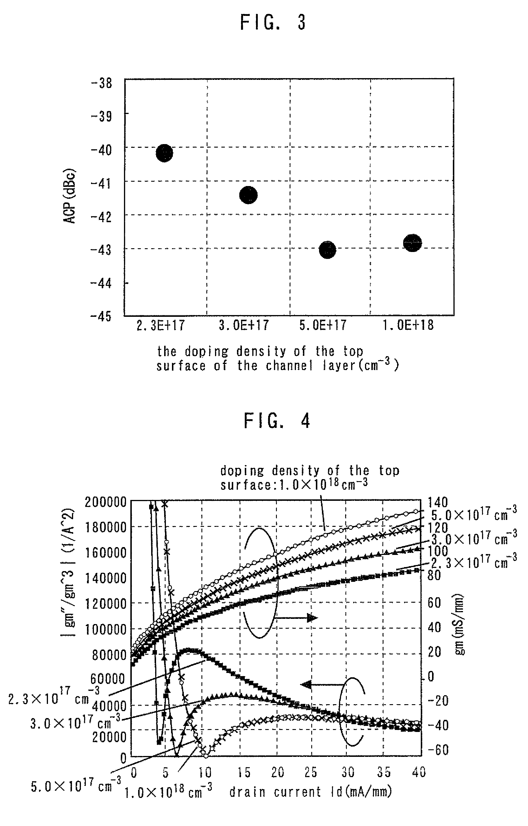
[0044]A second embodiment of the present invention provides a semiconductor device in which the channel layer has a graded doping profile such that the dopant impurity concentration varies inversely with the third power of depth into the channel layer from the top surface of the channel layer, as in the semiconductor device of the first embodiment. The gate electrode (21) of this semiconductor device has a gate length Lg of 0.2 μm-0.6 μm. Unlike the first embodiment, the doping impurity concentration at the top surface of the channel layer is not limited to any particular range. The following example assumes that the channel layer has a thickness of 700 Å and its top surface has a doping density of 5.0×1017 cm−3. Except for the features described above, the semiconductor device of the present embodiment is similar to that of the first embodiment. Further, it is manufactured in the same manner as described in connection with the first embodiment.
[0045]Characteristics of the semicondu...
third embodiment
[0051]FIG. 7 is a cross-sectional view of a semiconductor device according to a third embodiment of the present invention. This semiconductor device differs from that shown in FIG. 1 in that it includes an undoped Al0.20Ga0.80As buffer layer 22 (referred to simply as a “buffer layer” in the appended claims) instead of the undoped GaAs buffer layer 13 (also referred to as a “buffer layer” in the appended claims). It should be noted that undoped Al0.20Ga0.80As, from which the buffer layer 22 is formed, has a lower electron affinity than GaAs, from which the n-type GaAs channel layer 14 (referred to simply as a “channel layer” in the appended claims) is formed. Unlike the first embodiment, the doping density of the top surface of the channel layer is not limited to any particular range. Except for the features described above, the semiconductor device of the present embodiment is similar to that of the first embodiment. Further, the device is manufactured in the same manner as describe...
PUM
 Abstract
Description
Claims
Application Information
 - R&D
- Intellectual Property
- Life Sciences
- Materials
- Tech Scout
- Unparalleled Data Quality
- Higher Quality Content
- 60% Fewer Hallucinations
Browse by: Latest US Patents, China's latest patents, Technical Efficacy Thesaurus, Application Domain, Technology Topic, Popular Technical Reports.
© 2025 PatSnap. All rights reserved.Legal|Privacy policy|Modern Slavery Act Transparency Statement|Sitemap|About US| Contact US: help@patsnap.com


