
High second bit operation window method for virtual ground array with two-bit memory cells

a virtual ground array and memory cell technology, applied in the field of nonvolatile flash memory, can solve the problems of two-bit per cell nvm semiconductor devices, and achieve the effect of reducing the second bit effect and increasing the window of operation of the two-bit cell

Active Publication Date: 2011-07-26
MACRONIX INT CO LTD
View PDF13 Cites 0 Cited by
  • Summary
  • Abstract
  • Description
  • Claims
  • Application Information

AI Technical Summary

Benefits of technology

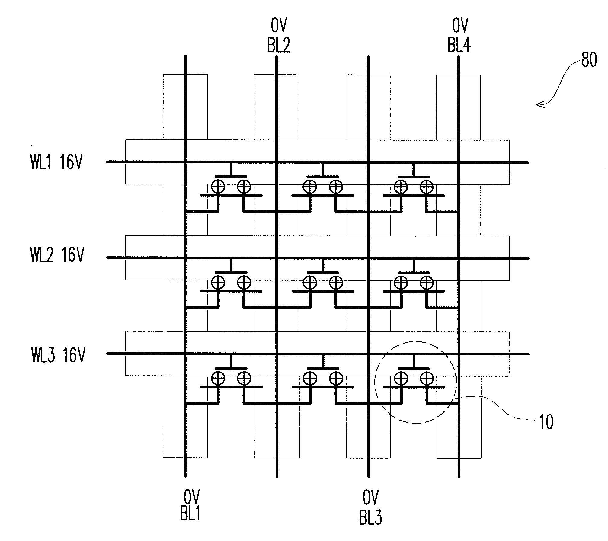
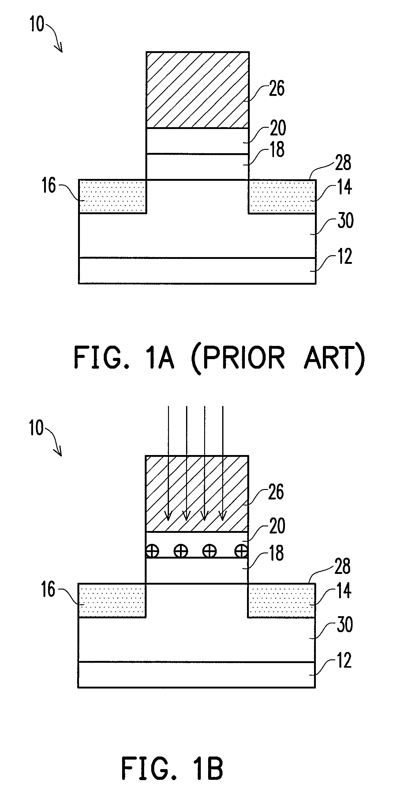
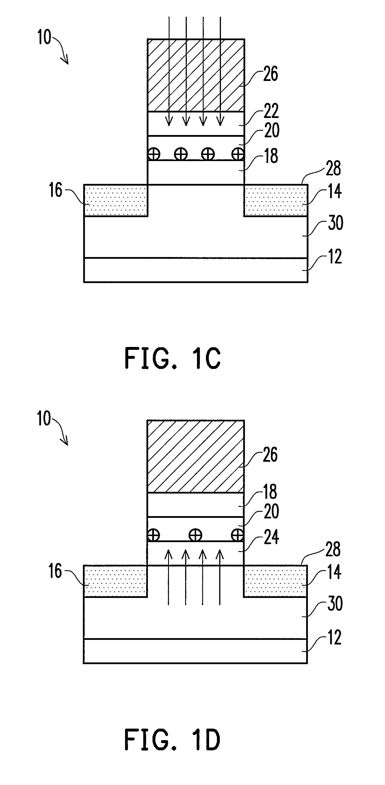
The present invention relates to a method for reducing the second bit effect on a two-bit NVM cell and increasing its window of operation. The method involves a Turn-On-Mode operation that lowers the initial voltage threshold of both bits to reduce the effect of programming one bit on the other. The method includes steps of erasing the cells, programming the bits, and reading the cells. The technical effect of the invention is to improve the reliability and performance of two-bit NVM cells in a virtual ground array.

Problems solved by technology

A limitation with two-bits per cell NVM semiconductor devices is a narrow “window of operation” that exists after the conventional programming of a two-bit cell.

Method used


Image

  • High second bit operation window method for virtual ground array with two-bit memory cells
  • High second bit operation window method for virtual ground array with two-bit memory cells
  • High second bit operation window method for virtual ground array with two-bit memory cells

Examples


Embodiment Construction

[0037]Certain terminology is used in the following description for convenience only and is not limiting. The words “right”, “left”, “lower”, and “upper” designate directions in the drawings to which reference is made. The words “inwardly” and “outwardly” refer to directions toward and away from, respectively, the geometric center of the object described and designated parts thereof. Their terminology includes the words above specifically mentioned, derivatives thereof and words of similar import. Additionally, the word “a” and the word “an”, as used in the claims and in the corresponding portions of the specification, means “at least one.”

[0038]As used herein, reference to conductivity will be limited to the embodiment described. However, those skilled in the art know that p-type conductivity can be switched with n-type conductivity and the device would still be functionally correct (i.e., a first or second conductivity type). Therefore, where used herein, the reference to n or p ca...


PUM


Abstract

A non-volatile VG memory array employing memory semiconductor cells capable of storing two bits of information having a non-conducting charge trapping dielectric, such as silicon nitride, layered in associating with at least one electrical insulating layer, such as an oxide, is disclosed. Bit lines of the memory array are capable of transmitting positive voltage to reach the source / drain regions of the memory cells of the array. A method that includes the hole injection erasure of the memory cells of the array that lowers the voltage threshold of the memory cells to a value lower than the initial voltage threshold of the cells is disclosed. The hole injection induced lower voltage threshold reduces the second bit effect such that the window of operation between the programmed and un-programmed voltage thresholds of the bits is widened. The programming and read steps reduce leakage current of the memory cells in the array.

Description

BACKGROUND OF THE INVENTION[0001]The present invention relates to non-volatile flash memory (“NVM”) semiconductor device which is able to continually store information even when the supply of electricity is removed from the device containing the NVM cell. More particularly, the invention relates to a NVM semiconductor device having two-bits per cell employed in a virtual ground (VG) array. Also, the invention relates to a method for programming the two-bits per cell NVM semiconductor in the VG array. This innovation provides for a more capable VG array due to the doubled memory density per cell, which is also known as multi-level flash memory. The invention also impacts an NVM semiconductor device “window of operation” that permits more effective use of two-bits per cell NVM semiconductor devices. The invention also addresses the leakage current issue experienced with VG arrays when some erasing, programming, and reading methods are applied.[0002]Multi-level, or multi-bit, flash mem...

Claims


Application Information

Patent Timeline
Patent Type & Authority Patents(United States)
IPC IPC(8): G11C16/04H10B69/00
CPCG11C16/0475G11C16/0491H01L21/28282H01L27/11568H01L29/7923H01L29/40117H10B43/30
Inventor WU, CHAO-I
Owner MACRONIX INT CO LTD
Learn More