Method of driving field emission device (FED) and method of aging FED using the same

a field emission device and a technology for aging field emission display apparatus, which are applied in the direction of discharge tube cold cathodes, instruments, discharge tube main electrodes, etc., can solve the problems of high possibility of arcing during the aging process, easy arcing between electrostatic particles, and plurality of feds of field emission display apparatus including a plurality of feds

Inactive Publication Date: 2011-07-05
SAMSUNG ELECTRONICS CO LTD
View PDF27 Cites 2 Cited by
  • Summary
  • Abstract
  • Description
  • Claims
  • Application Information

AI Technical Summary

Benefits of technology

[0014]It is yet another object to provide a method for preventing arcing when a field emission device (FED) is driven and for improving uniformity of electron emission of an apparatus including a plurality of FEDs.
[0015]It is still another object to provide a method for reducing the effect of a hot spot and activating a dead spot when the apparatus including the plurality of FEDs is aged.

Problems solved by technology

When the driving voltage is powered on, a voltage drop between the cathode electrode and the anode electrode remains constant, so that a lot of electrostatic particles gather around a tip of the electron emission source, which may cause arcing between the electrostatic particles.
In particular, when the driving voltage is either powered off from a power-on state or powered-on from a power-off state, overshoot occurs, which is more likely to cause arcing.
Furthermore, a field emission display apparatus including a plurality of FEDs can easily obtain inconstant light emission such as a hot spot and a dead spot due to a small non-uniform difference between a plurality of tips of the electron emission source.
The contemporary method for driving FEDs causes a high possibility of arcing during the aging process, and undesirably maintains the hot spot or the dead spot after the aging process is completed.

Method used


Image

  • Method of driving field emission device (FED) and method of aging FED using the same
  • Method of driving field emission device (FED) and method of aging FED using the same
  • Method of driving field emission device (FED) and method of aging FED using the same

Examples


Embodiment Construction

[0036]The present invention will now be described more fully with reference to the accompanying drawings in which exemplary embodiments of the invention are shown. Like reference numerals refer to like elements throughout the drawings. In the drawings, the thickness of layers and regions are exaggerated for clarity.

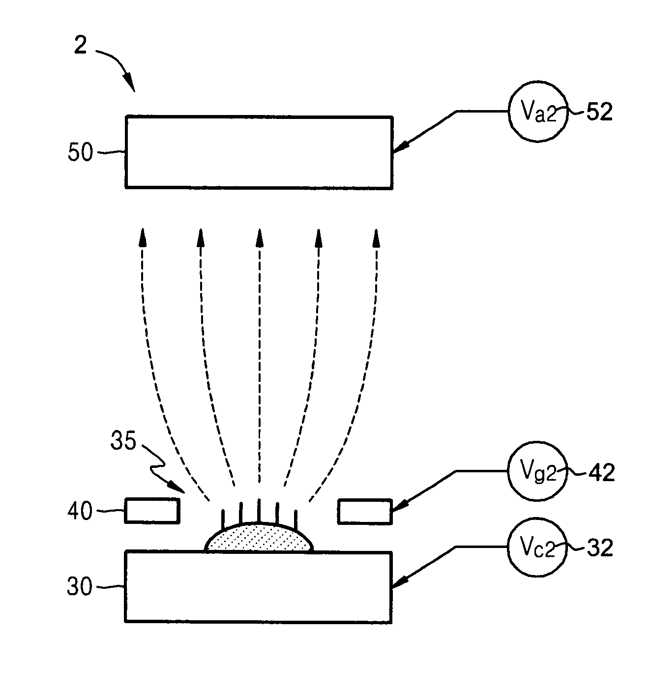
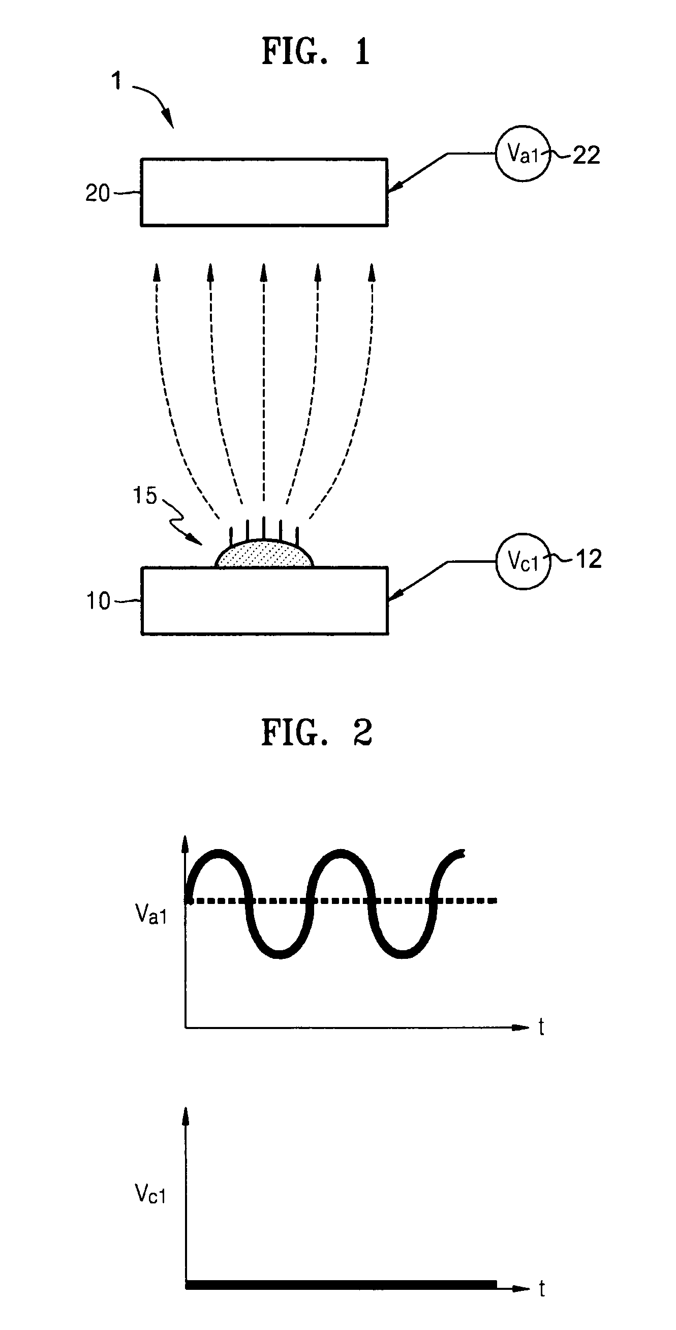
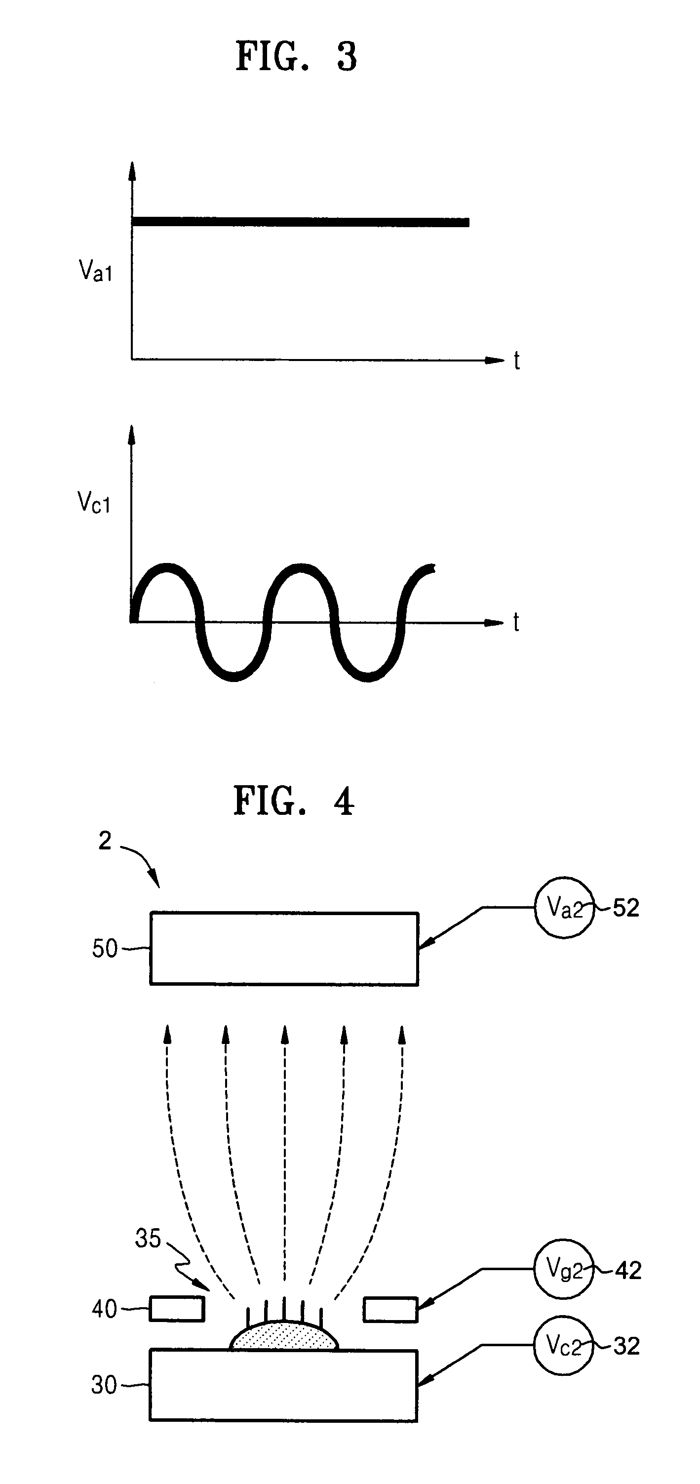
[0037]FIG. 1 illustrates a two-electrode structure field emission device (FED). FIGS. 2 and 3 are graphs illustrating driving voltages for the two-electrode structure FED illustrated in FIG. 1 according to embodiments of the principles of the present invention.

[0038]According to FIG. 1, a two-electrode structure FED 1 is constructed with a cathode electrode 10 including an emitter 15, and an anode electrode 20 facing cathode electrode 10. Vc1 denotes a driving voltage for cathode electrode 10. Terminal of the cathode driving circuit is 12. Va1 denotes a driving voltage for anode electrode 20. Terminal of the anode driving circuit is 22. Referring to FIG. 2, a constant vol...


PUM


Abstract

A method for driving a field emission device (FED) applies an alternating (AC) voltage as a driving voltage for emitting electrons in a field emission device comprising cathode electrode including an emitter and an anode electrode facing the cathode electrode. A method for aging an FED uses a constant voltage so that electrons cannot be emitted from the electron emission source, and an AC voltage so that electrons can be periodically emitted from the emitter when the FED is aged.

Description

CLAIM OF PRIORITY[0001]This application makes reference to, incorporates the same herein, and claims all benefits accruing under 35 U.S.C. §119 from an application for DRIVING METHOD OF FIELD EMISSION DEVICE AND AGING METHOD USING THE SAME earlier filed in the Korean Intellectual Property Office on 3 May 2006 and there duly assigned Serial No. 10-2006-0040082.BACKGROUND OF THE INVENTION[0002]1. Field of the Invention[0003]The present invention relates to a method for driving a field emission device (FED) and a method for aging a field emission display apparatus using the same, and more particularly, to a method for preventing arcing by applying an alternating (AC) voltage as a driving voltage to an FED and improving uniformity of electron emission of a field emission display apparatus comprising a plurality of FEDs.[0004]2. Description of the Related Art[0005]Field emitter array (FEA) type electron emission devices, surface conduction emitter (SCE) type electron emission devices, me...

Claims


Application Information

Patent Timeline
Patent Type & Authority Patents(United States)
IPC IPC(8): G09G3/20
CPCG09G3/32G09G3/2014G09G2310/0256G09G2310/066G09G2320/043G09G3/20G09G3/22H01J1/30
Inventor BAIK, CHAN-WOOKLEE, JEONG-HEEHEO, JEONG-NACHUNG, DEUK-SEOKJEONG, TAE-WONMIN, KYOUNG-WON
Owner SAMSUNG ELECTRONICS CO LTD
Why Eureka
Try Eureka