Light source device, having wavelength conversion and separation means, and projector
a technology of wavelength conversion and separation means and light source devices, which is applied in the direction of discharge tube luminescnet screens, lighting and heating apparatus, transmission monitoring, etc., can solve the problems of difficult to achieve high wavelength conversion efficiency with a simple and small configuration, and increase optical loss, so as to reduce light emission and high wavelength conversion efficiency , the effect of effective light utilization
- Summary
- Abstract
- Description
- Claims
- Application Information
AI Technical Summary
Benefits of technology
Problems solved by technology
Method used
Image
Examples
first embodiment
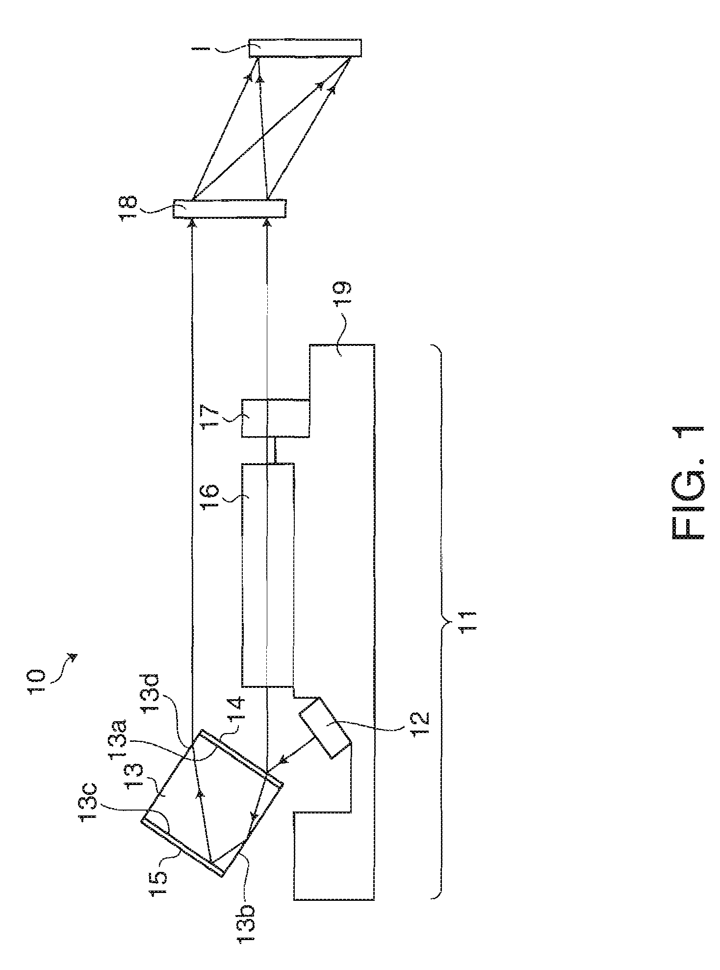
[0057]FIG. 1 is a diagram schematically illustrating a configuration of an illuminating device 10 according to a first embodiment of the invention. The illuminating device 10 includes a light source device and a diffusion element 18. The light source device 11 includes a semiconductor element 12, an optical prism 13, an SHG element 16, and an external resonator 17 which are disposed on a substrate 19. The semiconductor element 12 serves as a light source unit emitting a basic light of a first wavelength. The first wavelength is, for example, 1064 nm.
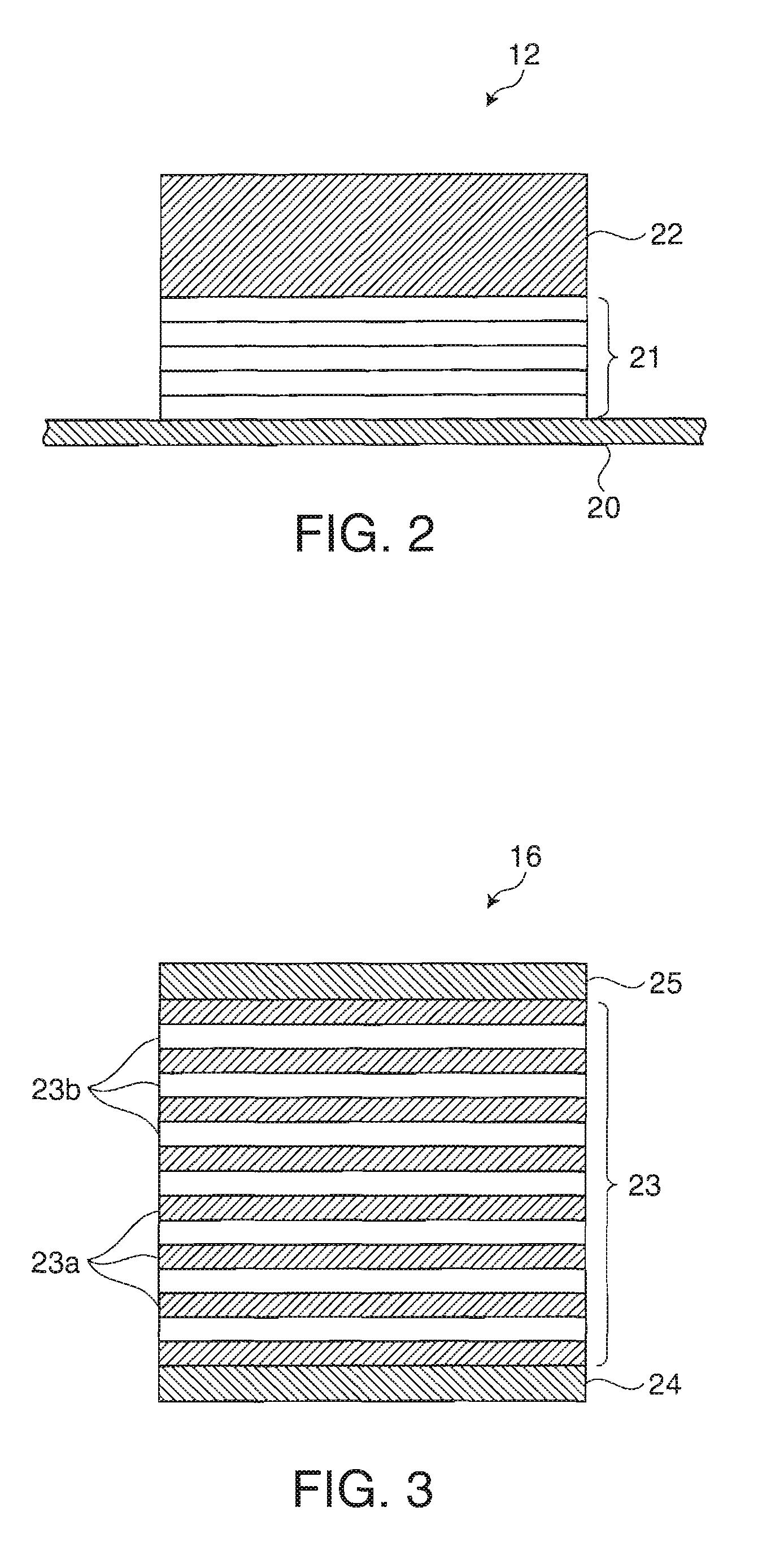
[0058]FIG. 2 is a diagram schematically illustrating a sectional configuration of the semiconductor element 12. The semiconductor element 12 is a so-called surface-emitting semiconductor element and has a substrate 20 formed of a semiconductor wafer, a mirror layer 21 that is formed on the substrate 20 to have a function of a reflecting mirror, and a laser medium 22 formed on the mirror layer 21.
[0059]The mirror layer 21 is formed on the...
second embodiment
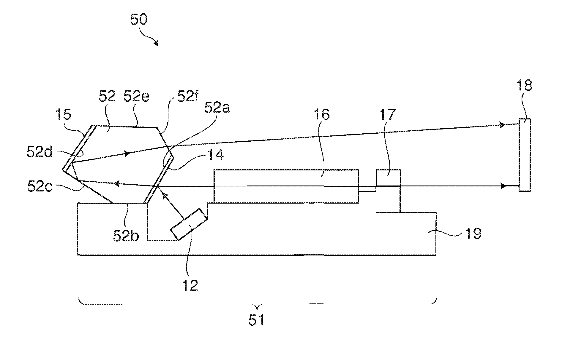
[0093]FIG. 15 is a diagram schematically illustrating a configuration of a light source device 100 used in an illuminating device according to a second embodiment of the invention. The light source device 100 includes an optical prim 101 having a pentagonal section. In the section of the optical prism 101, a fourth face 111d and a fifth face 101e form an obtuse angle. The same elements as the above-mentioned embodiment are denoted by the same reference numerals and repeated description thereof is omitted. In the above-mentioned embodiment, the semiconductor element 12 is disposed to be tilted about the face of the substrate 19 provided with the SHG element 16 or the face provided with the external resonator 17. On the contrary, in the second embodiment, a substrate 102 in which the semiconductor element 12 is disposed not to be tilted about the face provided with the SHG element 16 or the face provided with the external resonator 17 is used.
[0094]The optical prism 101 as an optical ...
third embodiment
[0098]FIG. 16 is a diagram schematically illustrating a configuration of a light source device 110 used in an illuminating device according to a third embodiment of the invention. The light source device 110 includes an optical prism 111 having a square-shaped section. The same elements as the above-mentioned embodiments are denoted by the same reference numerals and repeated description thereof is omitted. A first wavelength separating film 112 as a first wavelength separating section is formed on a first face 111a of the optical prism 111 as an optical element. The first wavelength separating film 112 serves as a wavelength separating section reflecting a part of the light of the first wavelength from the external resonator 17 and transmitting a part of the light of the first wavelength and the light of the second wavelength.
[0099]A second face 111b is a face adjacent to the first face 111a and is perpendicular to the first face 111a. A third face 111c is a face adjacent to the se...
PUM
 Abstract
Description
Claims
Application Information
 - R&D
- Intellectual Property
- Life Sciences
- Materials
- Tech Scout
- Unparalleled Data Quality
- Higher Quality Content
- 60% Fewer Hallucinations
Browse by: Latest US Patents, China's latest patents, Technical Efficacy Thesaurus, Application Domain, Technology Topic, Popular Technical Reports.
© 2025 PatSnap. All rights reserved.Legal|Privacy policy|Modern Slavery Act Transparency Statement|Sitemap|About US| Contact US: help@patsnap.com


