
Data processing apparatus and method thereof

a data processing apparatus and color space technology, applied in the field of data processing techniques in color space conversion of image data, can solve the problems of poor cost performance and large memory size, and achieve the effect of improving the cost performance of processing using lu

Inactive Publication Date: 2011-05-31
CANON KK
View PDF7 Cites 1 Cited by
  • Summary
  • Abstract
  • Description
  • Claims
  • Application Information

AI Technical Summary

Benefits of technology

The present invention aims to improve the cost performance of processing using an LUT (look-up table) and reduce the cache size while maintaining a high hit rate. It provides a data processing apparatus and method for generating a memory address and interpolating data read out from the first memory. The apparatus includes a selection unit, checking unit, transfer unit, determination unit, and change unit. The method involves selecting a part of the memory address, checking if the first memory stores data corresponding to the selected part, transferring the data from a second memory to the first memory, determining to change a part of the memory address based on the checking result, and changing the part to select a part of the memory address corresponding to characteristics of the memory address.

Problems solved by technology

In this case, the size of the LUT increases to the fourth power of the number of grids, thus requiring a huge memory size.
Hence, a problem of poor cost performance is posed.
Furthermore, such a problem is similarly posed when an LUT is used in processing other than color space conversion.

Method used


Image

  • Data processing apparatus and method thereof
  • Data processing apparatus and method thereof
  • Data processing apparatus and method thereof

Examples


first embodiment

1. Hardware Arrangement of Information Processing Apparatus

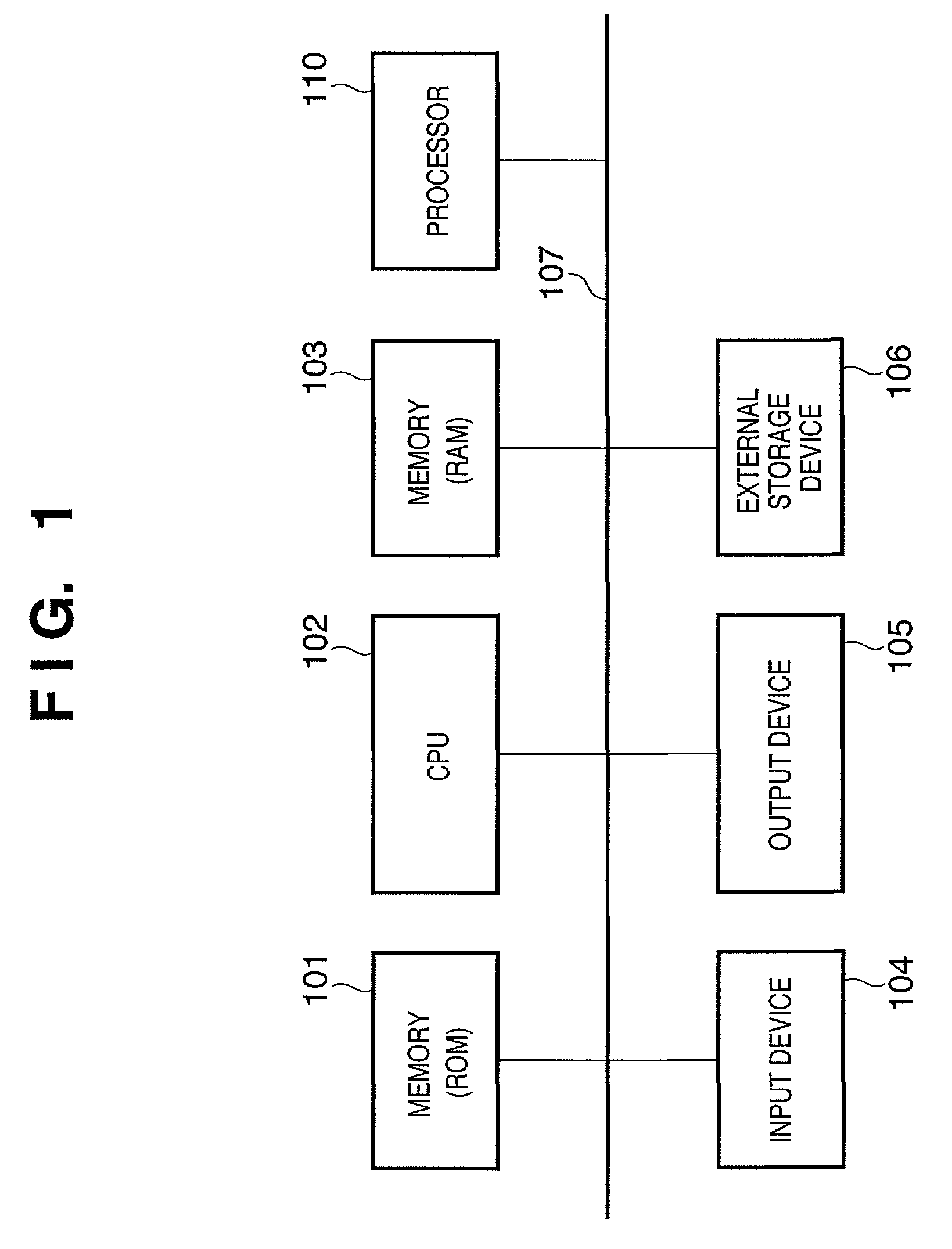
[0037]FIG. 1 is a block diagram showing the hardware arrangement of an information processing apparatus according to the first embodiment of the present invention.

[0038]Referring to FIG. 1, reference numeral 101 denotes a memory (ROM); 102, a CPU; 103, a memory (RAM); 104, an input device; 105, an output device; 106, an external storage device; and 107, a bus. The ROM 101 stores control programs required to implement the information processing functions according to this embodiment and data used in these control programs. These control programs and data are loaded onto the memory 103 as needed via the bus 107 under the control of the CPU 102, and are executed by the CPU 102. Reference numeral 110 denotes a processor which implements a color space conversion function and an LUT address conversion function, as will be described later.

[0039]The input device 104 is used to input various kinds of information. Assume that various ...

embodiment

5. Embodiment

[0081]An embodiment of the LUT address conversion processing in the information processing apparatus according to this embodiment will be described below. As an embodiment, an LUT address A1 output from the bit order converter 304 is defined as follows:[0082]LUT address A1=[b14, b13, b12, b11, b10, b9, b8, b7, b6, b5, b4, b3, b2, b1, b0]

[0083]Note that the number if ‘[ ]’ represents 1 bit, and ‘,’ represents bit concatenation to have the left end as the MSB and the right end as the LSB. Eight bits (b14, b13, . . . , b7) define the tag of the LUT address, and seven bits (b6, b5, . . . , b0) define the index of the LUT address.

[0084]FIG. 6 is a timing chart of the LUT address output from the bit order converter 304, and that stored in the address register 321. An LUT address A0 stored in the address register 321 at time n+1 in FIG. 6 is defined as follows:

[0085]LUT address A0=[r14, r13, r12, r11, r10, r9, r8, r7, r8, r5, r4, r3, r2, r1, r0]

[0086]Therefore, at time n+1, th...

second embodiment

[0094]The first embodiment generates the address conversion signal from all bits (e.g., 15 bits) of the LUT address. However, the present invention is not particularly limited to this.

[0095]For example, in a mode of filling a cache in a predetermined unit (to be referred to as a “line” hereinafter) to improve the fill efficiency of the cache, the number of entries of a tag memory that stores cache tags can be reduced. For example, if the predetermined unit is “16”, b=4, and lower 4 bits are reduced from the address input of the tag memory (such bits will be referred to as burst bits hereinafter).

[0096]Hence, the LUT address excluding the burst bits may be input to the LUT address comparator 302. That is, the contents of an address register having the bit width of the LUT address excluding the burst bits may be compared with the LUT address excluding the burst bits, and an address conversion signal may be generated based on the change frequency counters 311 as many as the number of b...


PUM


Abstract

A data processing apparatus generates a memory address corresponding to a first memory, and interpolates data read out from the first memory. The data processing apparatus selects a part of the memory address, checks if the first memory stores data corresponding to the selected part of the memory address, and transfers the data, for which it is determined that the first memory does not store the data, and which corresponds to the part of the memory address, from a second memory to the first memory. The data processing apparatus determines to change a part to be selected of the memory address based on the checking result indicating that the first memory does not store the data corresponding to the selected part of the memory address, and changes the part of the memory address corresponding to the characteristics of the memory address.

Description

BACKGROUND OF THE INVENTION[0001]1. Field of the Invention[0002]The present invention relates to a data processing technique in color space conversion of image data.[0003]2. Description of the Related Art[0004]In recent years, color input devices such as scanners, digital cameras, video cameras, and the like have prevailed as input devices. Also, various color output devices such as color printers using an ink-jet system, dye sublimation system, electrophotographic system, and the like have prevailed as output devices. These color input and output devices respectively have unique color spaces (device color spaces). In order to print data read by an input device using an output device, processing for converting the color space of the input device into that of the output device (to be referred to as “color space conversion” hereinafter) is required.[0005]For example, upon printing RGB image data scanned by a scanner, the RGB color space of the scanner is converted into a standard colo...

Claims


Application Information

Patent Timeline
Patent Type & Authority Patents(United States)
IPC IPC(8): G06F12/00
CPCG06F12/0895
Inventor TSUTSUMI, TAKAYUKI
Owner CANON KK
Learn More