
Solar cell containing silicon and chalcopyrite semiconductor layers

a technology of chalcopyrite and silicon, applied in the field of solar cells, can solve the problems of increased solar cell production cost, disadvantageous silicon semiconductor layer, poor light-absorbing efficiency, etc., and achieve the effect of enhancing light-absorbing efficiency

Inactive Publication Date: 2011-04-05
NEXPOWER TECH
View PDF6 Cites 6 Cited by
  • Summary
  • Abstract
  • Description
  • Claims
  • Application Information

AI Technical Summary

Benefits of technology

[0007]Accordingly, the present invention is directed to a solar cell for enhancing light-absorbing efficiency.
[0008]The present invention is also directed to a solar cell for reducing fabrication difficulty.
[0009]The present invention is further directed to a solar cell for decreasing production cost.
[0010]The present invention is further directed to a solar cell for enhancing light-absorbing efficiency without increasing the thickness of an intrinsic semiconductor layer.
[0011]The present invention is further directed to a solar cell for reducing the thickness of the solar cell.
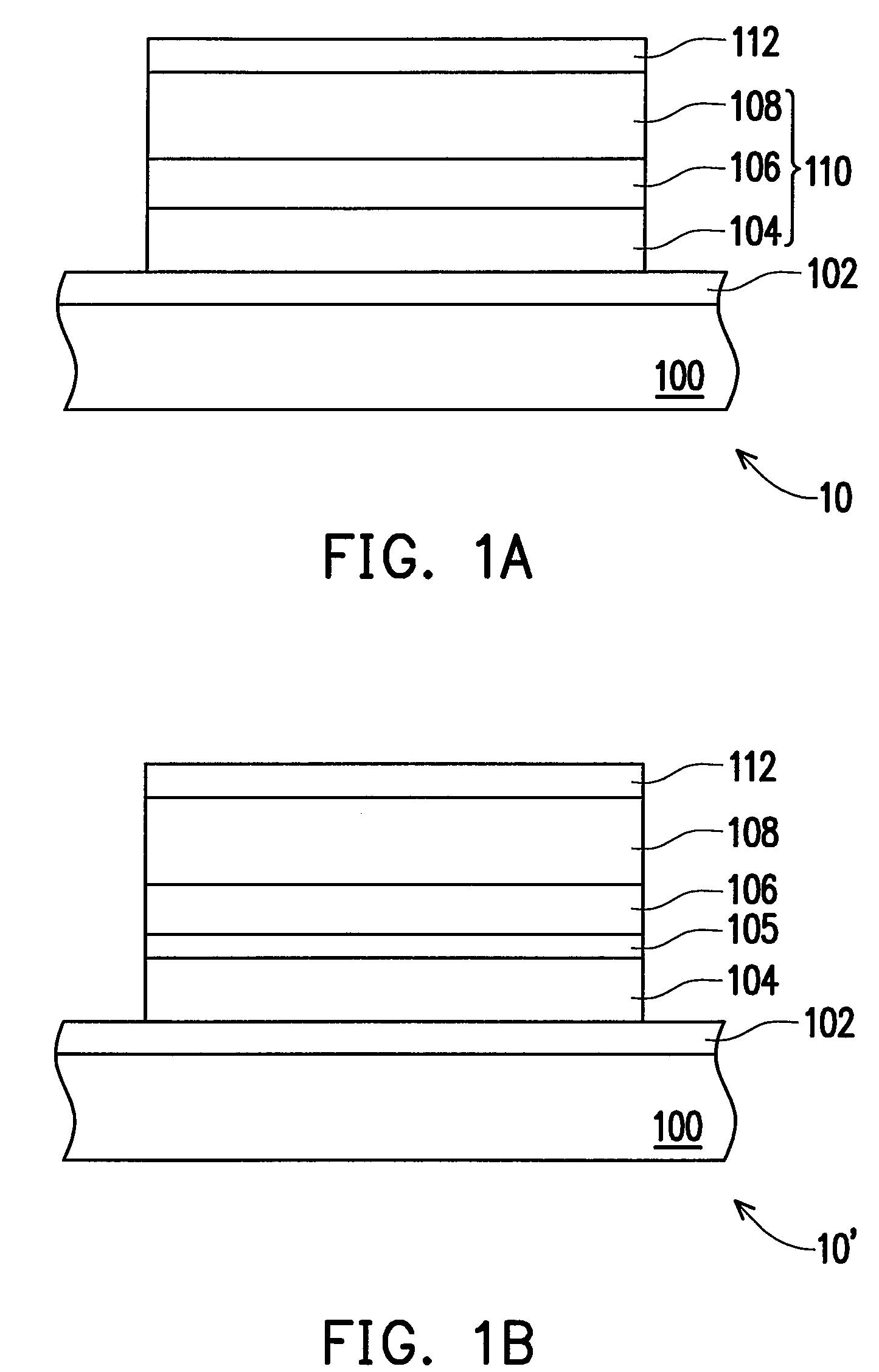
[0027]According to the present invention, chalcopyrite is used to form the intrinsic semiconductor layer. Consequently, the light-absorbing efficiency of the intrinsic semiconductor layer is higher than that of an intrinsic semiconductor layer formed by amorphous silicon. Thereby, the thickness of the intrinsic semiconductor layer in the present invention can also be reduced to achieve the purposes of lowering the production cost and enhancing the optical-electrical converting efficiency of the solar cell.

Problems solved by technology

However, the intrinsic semiconductor layer made of amorphous silicon is disadvantageous in poor light-absorbing efficiency.
However, as the thickness of the intrinsic semiconductor layer increases, the thickness of the solar cell is also increased, which raises the production cost thereof.
However, this method not only increases production cost and fabrication difficulty but increases internal resistance as well.
Therefore, in this method, the P-type semiconductor layer, the intrinsic semiconductor layer, and the N-type semiconductor layer are not unrestrictedly stacked to achieve the purpose of increasing light-absorbing efficiency.

Method used


Image

  • Solar cell containing silicon and chalcopyrite semiconductor layers
  • Solar cell containing silicon and chalcopyrite semiconductor layers
  • Solar cell containing silicon and chalcopyrite semiconductor layers

Examples


Embodiment Construction

[0037]FIG. 1A illustrates a cross-sectional view of a solar cell according to an embodiment of the present invention.

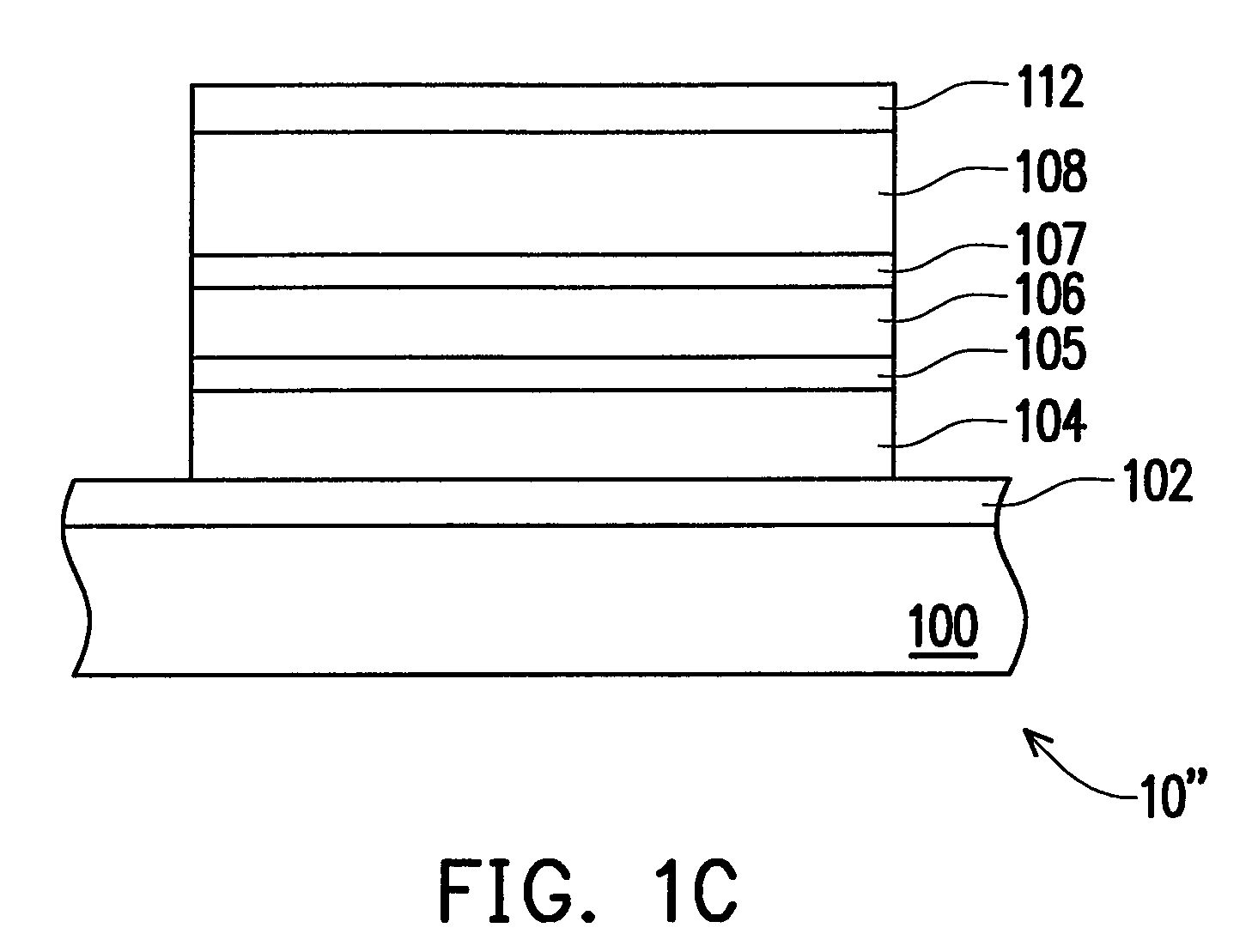
[0038]Referring to FIG. 1A, a solar cell 10 is disposed on a substrate 100. The solar cell 10 comprises an electrode 102, an electrode 112, and a stacked semiconductor layer 110. A material of the substrate 100 is, for example, glass. The electrode 112 is disposed on the substrate 100. A material of the electrode 112 is, for example, aluminum, silver or other alloys. A thickness of the electrode 112 is, for example, between 10 Å and 5000 Å. The electrode 102 is disposed between the substrate 100 and the electrode 112. A material of the electrode 102 is, for example, aluminum doped zinc oxide (AZO), gallium doped zinc oxide (GZO), SnO2, or transparent conductive oxide (TCO). A thickness of the electrode 102 is, for example, between 50 Å and 300 Å. The stacked semiconductor layer 110 is disposed between the electrodes 102 and 112. The stacked semiconductor layer 110 com...


PUM


Abstract

A solar cell includes a first electrode, a second electrode and a stacked semiconductor layer. The stacked semiconductor layer is disposed between the first electrode and the second electrode. The stacked semiconductor layer includes a first semiconductor layer, a second semiconductor layer and an intrinsic semiconductor layer. The first semiconductor layer has a first energy gap. The second semiconductor layer has a second energy gap. The intrinsic semiconductor layer is disposed between the first semiconductor layer and the second semiconductor layer, wherein the intrinsic semiconductor layer is a chalcopyrite layer and has a third energy gap. The third energy gap is less than the first energy gap and the second energy gap.

Description

BACKGROUND OF THE INVENTION[0001]1. Field of the Invention[0002]The present invention relates to a solar cell, and particularly relates to a solar cell with high light-absorbing efficiency and high optical-electrical converting efficiency, capable of lowering production cost and fabrication difficulty.[0003]2. Description of Related Art[0004]A solar cell has a very broad application spectrum appropriately covering electric power field (such as megawatts electric power generating system, home electric power generating system), communication field (such as wireless electric power, wireless communication), consumer electronic products (such as computer, watch, electric toy, radio receiver), traffic and transportation field (such as automobile, ship, traffic sign, road lighting, lighthouse), and agriculture field (such as water pump, irrigation).[0005]Usually, a solar cell is formed by stacking a P-type semiconductor layer, an intrinsic semiconductor layer and an N-type semiconductor la...

Claims


Application Information

Patent Timeline
Patent Type & Authority Patents(United States)
IPC IPC(8): H01L31/00
CPCH01L31/0322H01L31/075Y02E10/548Y02E10/541
Inventor LU, WEI-LUNHSIEH, FENG-CHIENTSENG, BAE-HENG
Owner NEXPOWER TECH
Learn More