
Dual gate FinFET

a technology of dual gate and finfet, which is applied in the direction of semiconductor devices, electrical apparatus, transistors, etc., can solve the problems of major limiting barrier to technology development, inability to further scale, and limited performance of integrated circuit devices in the sub 100 nm rang

Active Publication Date: 2011-03-01
INFINEON TECH AG
View PDF8 Cites 172 Cited by
  • Summary
  • Abstract
  • Description
  • Claims
  • Application Information

AI Technical Summary

Problems solved by technology

Integrated circuit device performance in the sub 100 nm range is often limited by short-channel effects.
Such short-channel effects make further scaling difficult if not impossible.
Challenges to the source-drain doping and requirement for scaled ultra shallow junctions which demand adequate doping abruptness with high doping activation, may be a major limiting barrier to technology development beyond the 65 nm range.

Method used


Image

  • Dual gate FinFET
  • Dual gate FinFET
  • Dual gate FinFET

Examples


Embodiment Construction

[0012]In the following description, reference is made to the accompanying drawings that form a part hereof, and in which is shown by way of illustration specific embodiments which may be practiced. These embodiments are described in sufficient detail to enable those skilled in the art to practice the invention, and it is to be understood that other embodiments may be utilized and that structural, logical and electrical changes may be made without departing from the scope of the present invention. The following description of example embodiments is, therefore, not to be taken in a limited sense, and the scope of the present invention is defined by the appended claims.

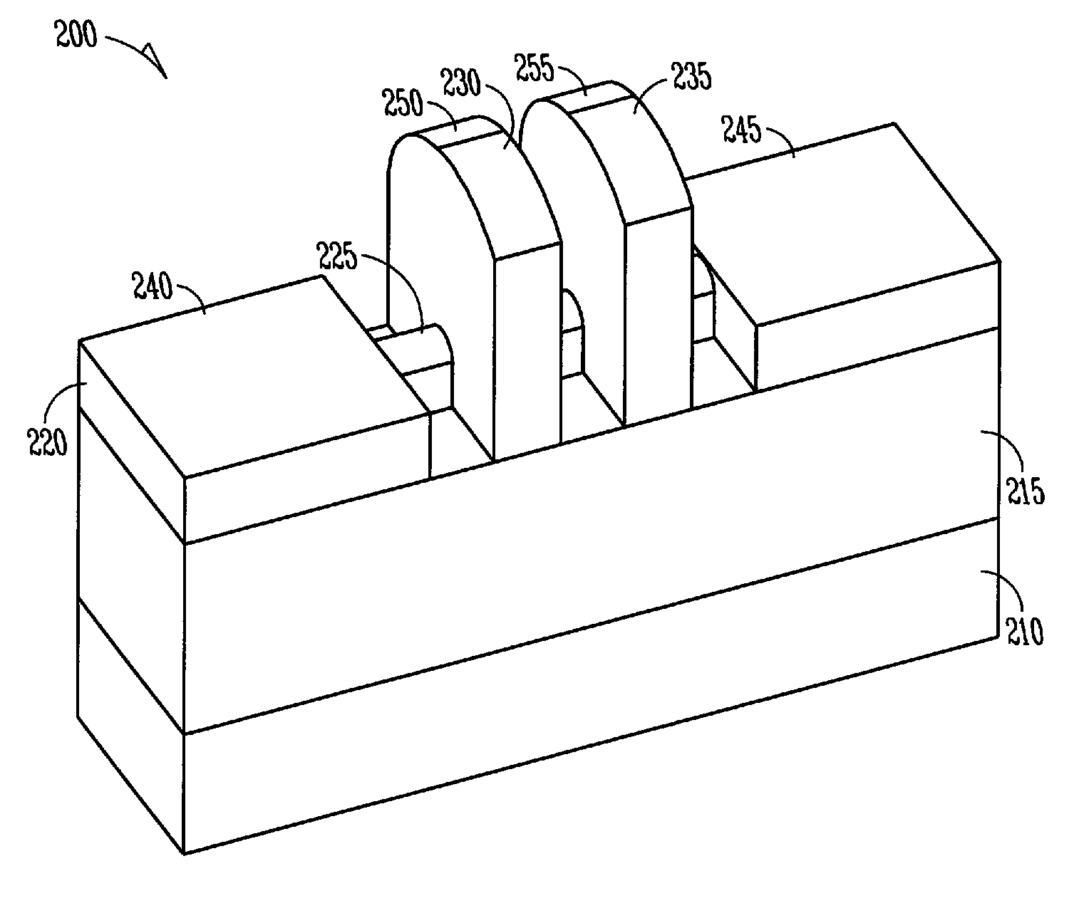
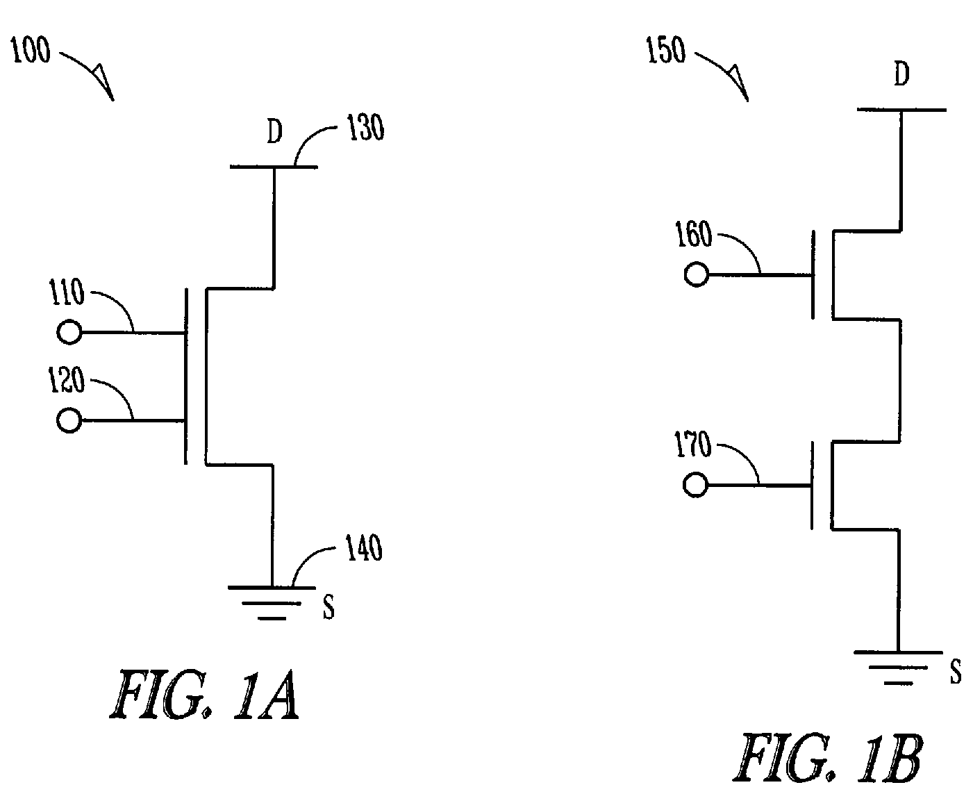
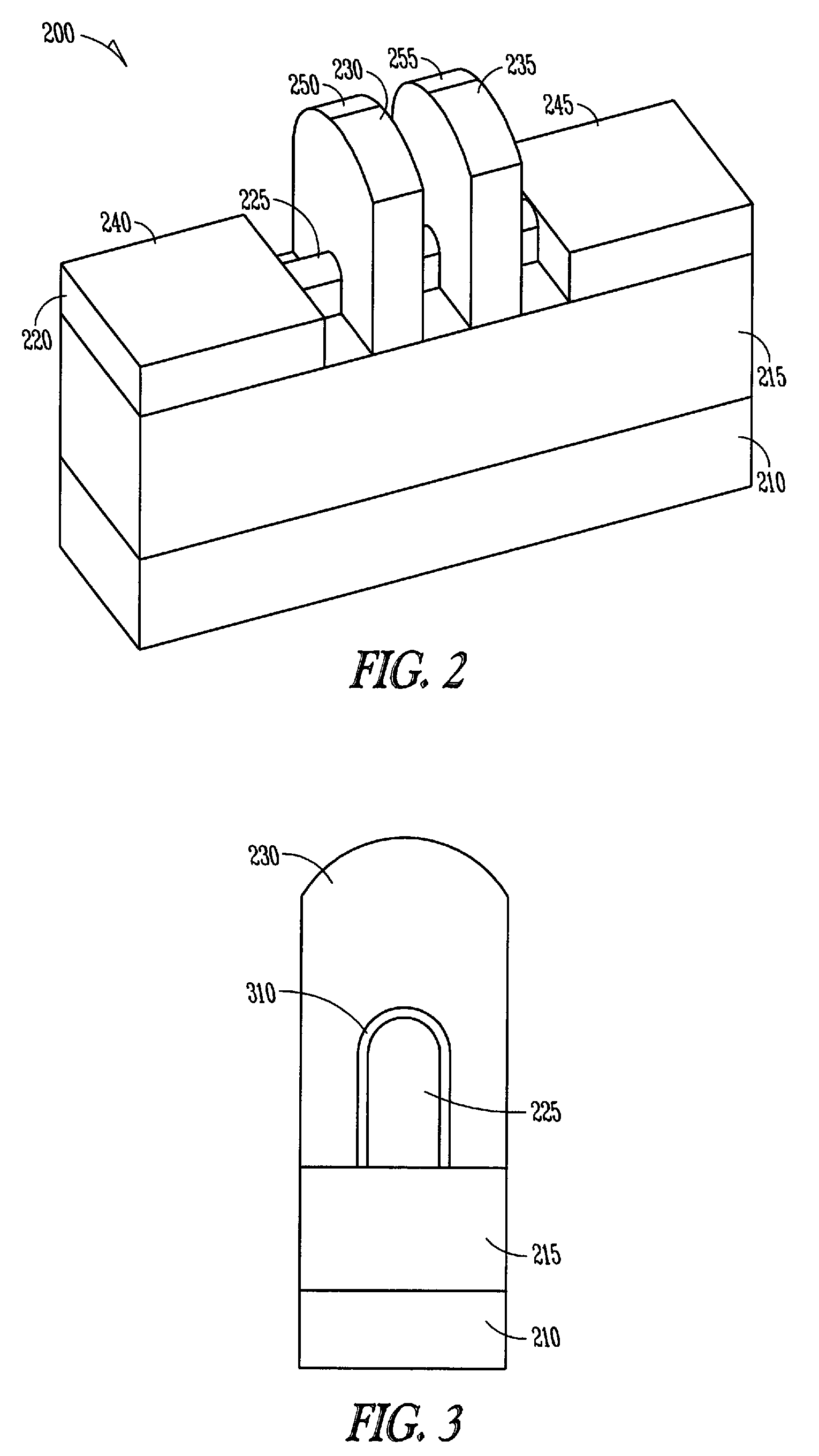
[0013]FIG. 1A is a circuit diagram of a dual gate FinFET (Fin type Field Effect Transistor) 100 according to an example embodiment. A first gate 110 and a second gate 120 are coupled to a channel between a drain 130 and source 140. In one embodiment, the gates 110 and 120 are independently accessible. Dual gate FinFET 10...


PUM


Abstract

A circuit has a fin supported by a substrate. A source is formed at a first end of the fin and a drain is formed at a second end of the fin. A pair of independently accessible gates are laterally spaced along the fin between the source and the drain. Each gate is formed around approximately three sides of the fin.

Description

BACKGROUND[0001]Integrated circuit device performance in the sub 100 nm range is often limited by short-channel effects. Such short-channel effects make further scaling difficult if not impossible. These effects are usually manifested as a reduction in transconductance, an increase in output conductance and a shift in the threshold voltage as transistor gate length is reduced.[0002]Another manifestation of short channel effects is an increase in the sub-threshold current. For low power or for high performance applications, tight control on the sub-threshold drain current and threshold voltage is needed. Challenges to the source-drain doping and requirement for scaled ultra shallow junctions which demand adequate doping abruptness with high doping activation, may be a major limiting barrier to technology development beyond the 65 nm range.BRIEF DESCRIPTION OF THE DRAWINGS[0003]FIG. 1A is a circuit diagram of a dual gate FinFET (Fin type Field Effect Transistor) according to an exampl...

Claims


Application Information

Patent Timeline
Patent Type & Authority Patents(United States)
IPC IPC(8): H01L29/78
CPCH01L29/66795H01L29/7854H01L29/78645
Inventor NAWAZ, MUHAMMAD
Owner INFINEON TECH AG
Learn More