Solid-state image sensors and display devices having anti-reflection film
a technology of solid-state image sensor and display device, which is applied in the direction of identification means, radiation controlled devices, instruments, etc., can solve the problems of high reflection loss, so as to achieve low sensitivity of solid-state image sensor and high reflectivity. , the effect of high reflection loss
- Summary
- Abstract
- Description
- Claims
- Application Information
AI Technical Summary
Benefits of technology
Problems solved by technology
Method used
Image
Examples
first embodiment
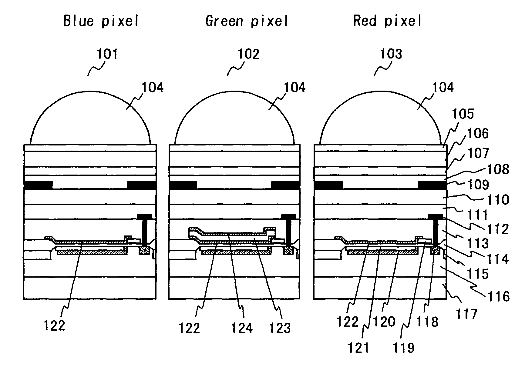
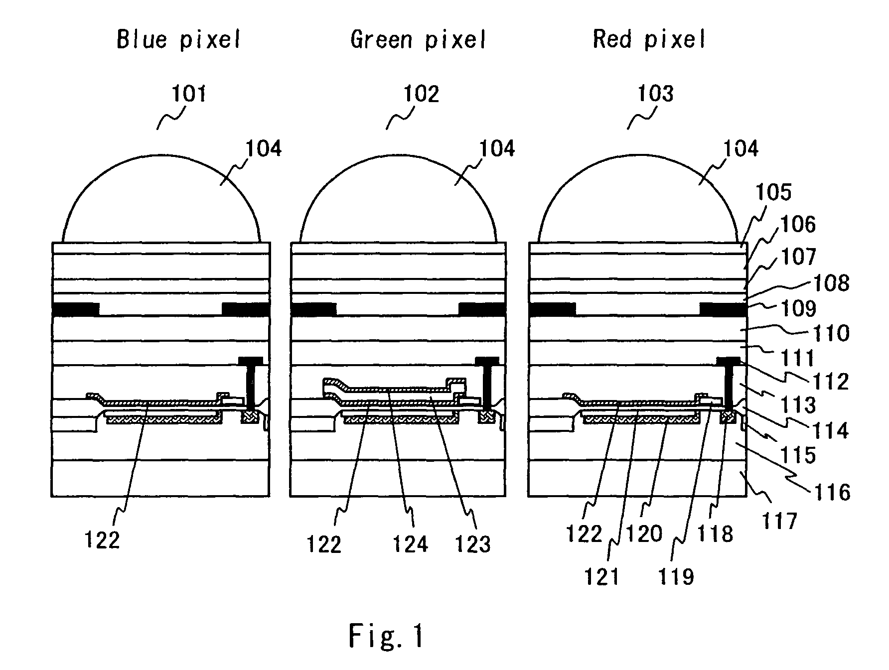
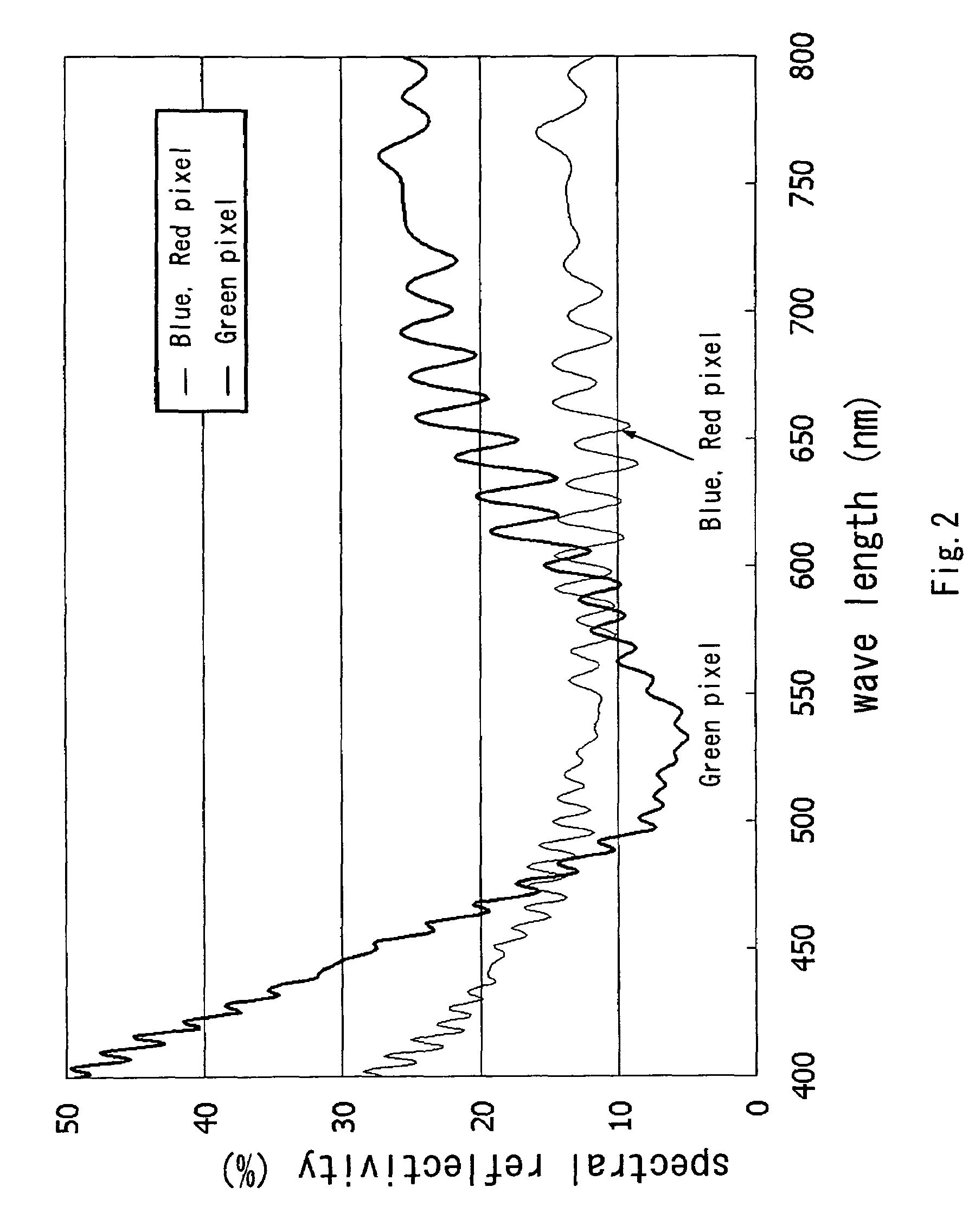
[0040]A first embodiment will be described with reference to FIG. 1. FIG. 1 shows an embodiment of a solid-state image sensor having an anti-reflection film including a single layer of high-refractive-index layer for the B pixel and R pixel and a double layer of high-refractive-index layers for the G pixel. FIG. 1 represents the cross sections cut at the previously described cutting positions A, B, and C of FIG. 7(b). In FIG. 1, reference numeral 101 represents the cross section of the B pixel when cut at the cutting position A; 102 represents the cross section of the G pixel when cut at the cutting position B; 103 represents the cross section of the R pixel when cut at the cutting position C; 104 represents a microlens; 105 and 107 represent planarizing layers; 106 represents a color filter; 108 represents a protection film; 109 represents a light-shielding film; 110, 111 and 113 represent interlayer insulation films; 112 represents aluminum wiring; 114 and 123 represent silicon ox...
second embodiment
[0056]Next, a second embodiment of the present invention is described in detail with reference to FIG. 3. FIG. 3 shows an embodiment of a solid-state image sensor having an anti-reflection film including a single layer of high-refractive-index layer for the B pixel and a double layer of high-refractive-index layers for the and R pixel and G pixel, and represents the cross sections cut at the previously described cutting positions A, B, and C of FIG. 7(b). In FIG. 3, reference numeral 101 represents the cross section of the B pixel when cut at the cutting position A, 102 represents the cross section of the G pixel when cut at the cutting position B, 303 represents the cross section of the R pixel when cut at the cutting position C, 125 represents a silicon oxide film forming a low-refractive-index layer having a refractive index of less than 1.7, and 126 represents a silicon nitride film forming a high-refractive-index layer having a refractive index of 1.7 or higher, respectively. S...
third embodiment
[0064]Next, a third embodiment of the present invention will be described in detail with reference to FIG. 5. FIG. 5 shows an embodiment of a solid-state image sensor having an anti-reflection film including a double layer of high-refractive-index layers for all the B pixel, G pixel, and R pixel, and represents the cross sections cut along the previously described cutting positions A, B, and C of FIG. 7(b). In FIG. 5, reference numeral 101 represents the cross section of the B pixel when cut at the cutting position A; 102 represents the cross section of the B pixel when cut at the cutting position B; 303 represents a cross section of the C pixel when cut at the cutting position C; 127 represents a silicon oxide film forming a low-refractive-index layer having a refractive index of less than 1.7; and 128 represents a silicon nitride film forming a high-refractive-index layer having a refractive index of 1.7 or higher, respectively. Since elements denoted by the same reference numeral...
PUM
| Property | Measurement | Unit |
|---|---|---|
| refractive index | aaaaa | aaaaa |
| refractive index | aaaaa | aaaaa |
| refractive index | aaaaa | aaaaa |
Abstract
Description
Claims
Application Information
 - R&D
- Intellectual Property
- Life Sciences
- Materials
- Tech Scout
- Unparalleled Data Quality
- Higher Quality Content
- 60% Fewer Hallucinations
Browse by: Latest US Patents, China's latest patents, Technical Efficacy Thesaurus, Application Domain, Technology Topic, Popular Technical Reports.
© 2025 PatSnap. All rights reserved.Legal|Privacy policy|Modern Slavery Act Transparency Statement|Sitemap|About US| Contact US: help@patsnap.com


