Receiving circuit and optical signal receiving circuit

a technology of receiving circuit and optical signal, which is applied in the direction of electromagnetic transceivers, gain control, pulse shaping, etc., can solve the problems of waveform distortion and significant difference in received power, and achieve accurate amplifying operation, wide dynamic range, and reduced load of the output portion of the transimpedance amplifier.

Inactive Publication Date: 2010-10-05
PANASONIC SEMICON SOLUTIONS CO LTD
View PDF8 Cites 5 Cited by
  • Summary
  • Abstract
  • Description
  • Claims
  • Application Information

AI Technical Summary

Benefits of technology

[0039]As described above, according to the present invention, only one comparison circuit is connected to the output portion of the transimpedance amplifier, so that the load of the output portion of the transimpedance amplifier can be reduced. Therefore, a light receiving circuit is provided in which, even when a high-speed response is performed, an accurate amplifying operation can be achieved with respect to an input optical or electrical signal having a wide dynamic range. Also, since only one comparison circuit is used, a configuration which provides a small area and low power consumption can be achieved.
[0040]Further, since a configuration is provided in which, even when an L-level data input is changed to an H-level data input, a high-speed response is obtained with respect to the H-level data after input of the L-level data. Therefore, it is possible to prevent an erroneous reaction to the L-level data input, resulting in an accurate AGC operation.
[0041]In addition, a high-speed response can be obtained with respect to input data input whose power is not constant and is gradually increased during, for example, a preamble period. Also in this case, an accurate AGC operation can be achieved.
[0042]With such a configuration, it is possible to provide a light receiving circuit which can address a wide dynamic range (i.e., from a small signal to a large signal), and receive data with high precision.
[0043]Further, according to the present invention, only two comparison circuits are used to adjust the output value of the transimpedance amplifier into an appropriate range, thereby making it possible to reduce the output load due to a small number of comparison circuits, perform a high-speed operation, and receive data with high precision due to accurate gain adjustment.

Problems solved by technology

In upward transmission from each subscriber to the station, the transmission distance from each subscriber to the station varies from subscriber to subscriber, resulting in a significant difference in received power.
However, in conventional light receiving circuits, when a large optical signal is input, the output of a transimpedance amplifier is saturated, so that a distortion occurs in a waveform.

Method used


Image

  • Receiving circuit and optical signal receiving circuit
  • Receiving circuit and optical signal receiving circuit
  • Receiving circuit and optical signal receiving circuit

Examples


first embodiment

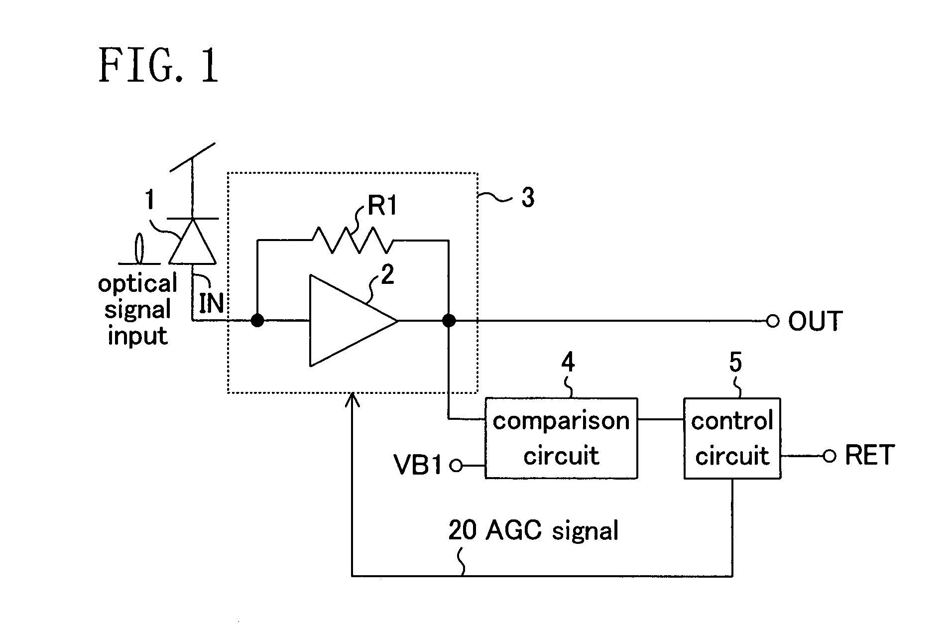
[0100]Initially, a first embodiment of a light receiving circuit of the present invention will be described with reference to FIG. 1.

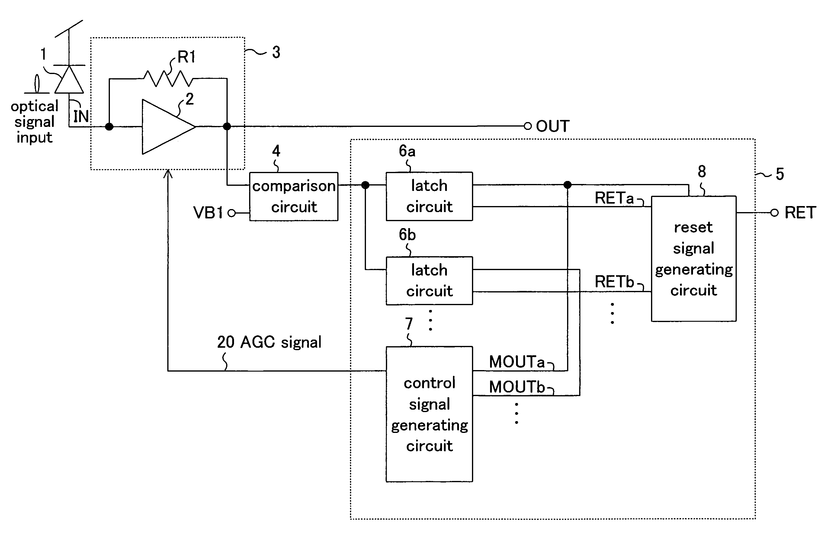
[0101]The light receiving circuit of FIG. 1 comprises: a light receiving element 1 for receiving an optical input signal and outputting a current proportional to the intensity of the input light; a transimpedance amplifier 3 comprising an inversion amplifier 2 for amplifying an electrical signal which is an output current obtained by photoelectric conversion of the light receiving element 1 and a feedback resistance R1 connected between an input IN and an output OUT of the inversion amplifier 2; a comparison circuit 4 for receiving an output of the transimpedance amplifier 3, comparing the output with a reference value (first comparative value) VB1 which is set to have a certain desired value to determine the level of the output of the transimpedance amplifier 3, and outputting the comparison result; and a control circuit 5 for holding the comparison r...

second embodiment

[0182]Next, a second embodiment of the receiving circuit of the present invention will be described with reference to FIG. 8.

[0183]The receiving circuit of this embodiment in which a register circuit is used to successively hold the comparison result of the comparison circuit 4, is different from that of the first embodiment in which the control circuit 5 of the receiving circuit uses the latch circuit to hold the comparison result of the comparison circuit 4.

[0184]Here, parts other than the register circuit have been described in the first embodiment, and therefore, the same parts will not be described.

[0185]A control circuit 5 included in the receiving circuit of this embodiment of FIG. 8 comprises: shift register circuits 11a, 11b, . . . for successively holding a comparison result output from a comparison circuit 4; and a control signal generating circuit 7 for generating an AGC signal 20 which is a control signal for adjusting the gain of a transimpedance amplifier 3 based on o...

third embodiment

[0193]Next, a third embodiment of the receiving circuit of the present invention will be described with reference to FIG. 9.

[0194]The receiving circuit of this embodiment of FIG. 9 is different from that of the first embodiment in that a reference value generating circuit 12 for generating an intermediate value of the output of the transimpedance amplifier 3, and a differential amplification circuit 13 for receiving the output of the transimpedance amplifier and the output of the reference value generating circuit 12 to generate a differential signal, are further provided.

[0195]When a differential signal is required in a subsequent amplifier circuit (e.g., in data communication, etc.), since the output signal OUT is a single signal in the configuration of the first embodiment of the present invention, single-differential conversion as described in the present invention is required.

[0196]Also, the reference value generating circuit 12 can be initialized by inputting a reset signal (i...


PUM


Abstract

A receiving circuit comprises a transimpedance amplifier 3 including an inversion amplifier 2 for amplifying an input current IN, and a feedback resistance R1 connected between an input and an output of the inversion amplifier 2, a comparison circuit 4 for comparing an output OUT of the transimpedance amplifier 3 with a certain desired reference value, and outputting a result of the comparison, and a control circuit for holding the comparison result, and generating an AGC signal 20 for adjusting a gain of the transimpedance amplifier 3. The transimpedance amplifier 20 has a function capable of gain adjustment in accordance with the input AGC signal 20. The control circuit 5 performs gain adjustment until the output OUT of the transimpedance amplifier 3 exceeds the reference value so that an appropriate gain is obtained. Therefore, even when an input has a wide dynamic range, it is possible to prevent signal saturation and a distortion in output waveform in the transimpedance amplifier, so that appropriate reception can be invariably performed and a signal having a stable duty can be output.

Description

RELATED APPLICATIONS[0001]This application is the U.S. National Phase under 35 U.S.C. §371 of International Application No. PCT / JP2005 / 015638 filed on Aug. 29, 2005, which in turn claims the benefit of Japanese Application No. 2004-259380, filed on Sep. 7, 2004, the disclosures of which Applications are incorporated by reference herein.TECHNICAL FIELD[0002]The present invention relates to a receiving circuit and a light receiving circuit which achieve a wide dynamic range.BACKGROUND ART[0003]In recent years, as information and communication technologies progress, there is a demand for higher-speed optical transmission, a larger transmission capacity, and a longer transmission distance, which require a considerably advanced transmission technique. A form of such an optical transmission technique is a PON (Passive Optical Network) system. In the PON system, one station and a plurality of subscribers are connected by time-division multiplexing. In upward transmission from each subscrib...

Claims


Application Information

Patent Timeline
Patent Type & Authority Patents(United States)
IPC IPC(8): H04B10/06H03F3/08H03G3/20H03K5/01H04B10/07H04B10/40H04B10/50H04B10/524H04B10/564H04B10/58H04B10/60H04B10/69
CPCH03F1/08H03F3/08H03G3/3084H03F2200/78
Inventor NISHIMURA, KAZUKOKIMURA, HIROSHI
Owner PANASONIC SEMICON SOLUTIONS CO LTD
Why Eureka
Try Eureka