Frame pulse signal latch circuit and phase adjustment method
a latch circuit and frame pulse technology, applied in the direction of pulse technique, generating/distributing signals, instruments, etc., can solve the problems of long adjustment time, process carried out, and the latch circuit cannot generate the original frame pulse signal
- Summary
- Abstract
- Description
- Claims
- Application Information
AI Technical Summary
Benefits of technology
Problems solved by technology
Method used
Image
Examples
first embodiment
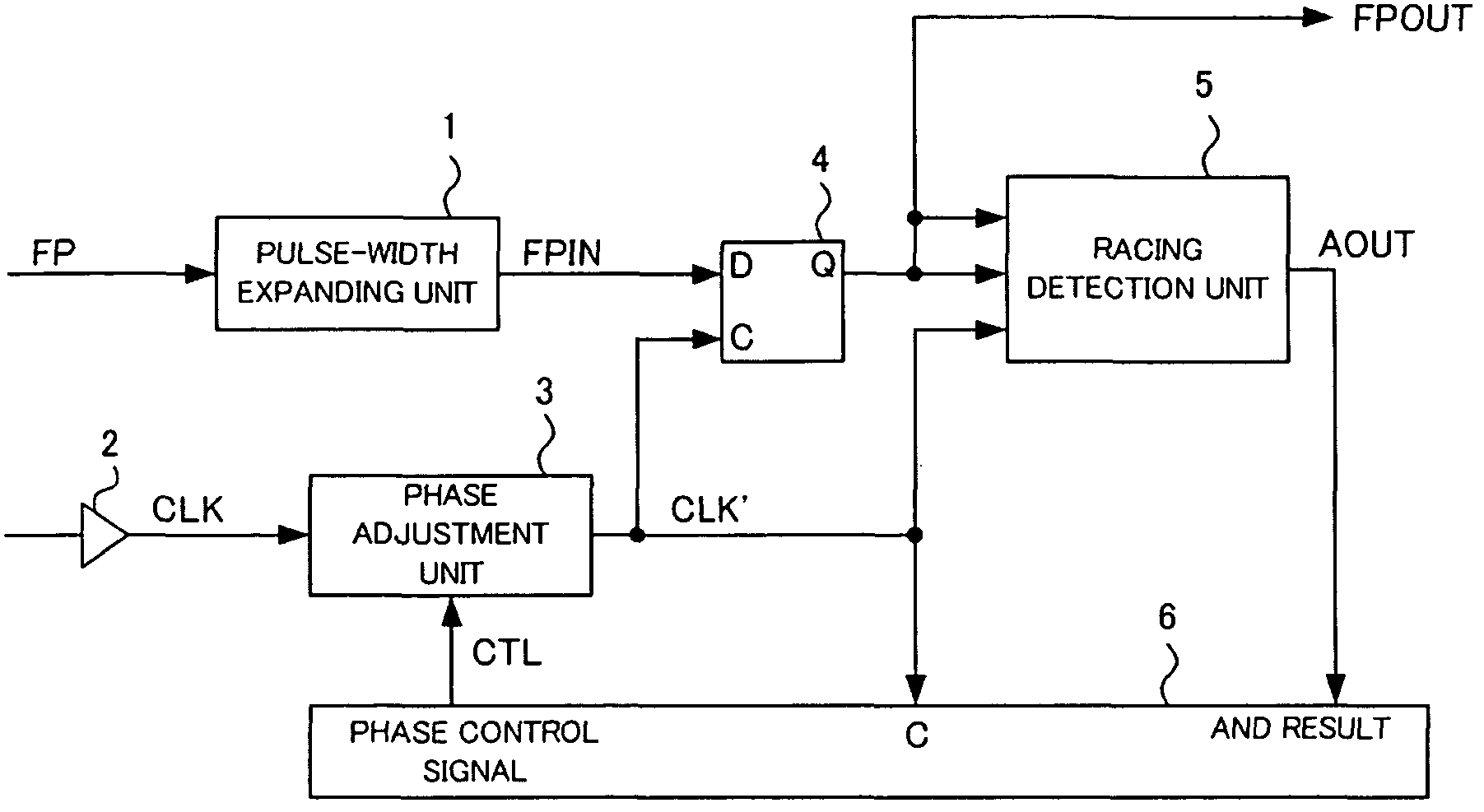
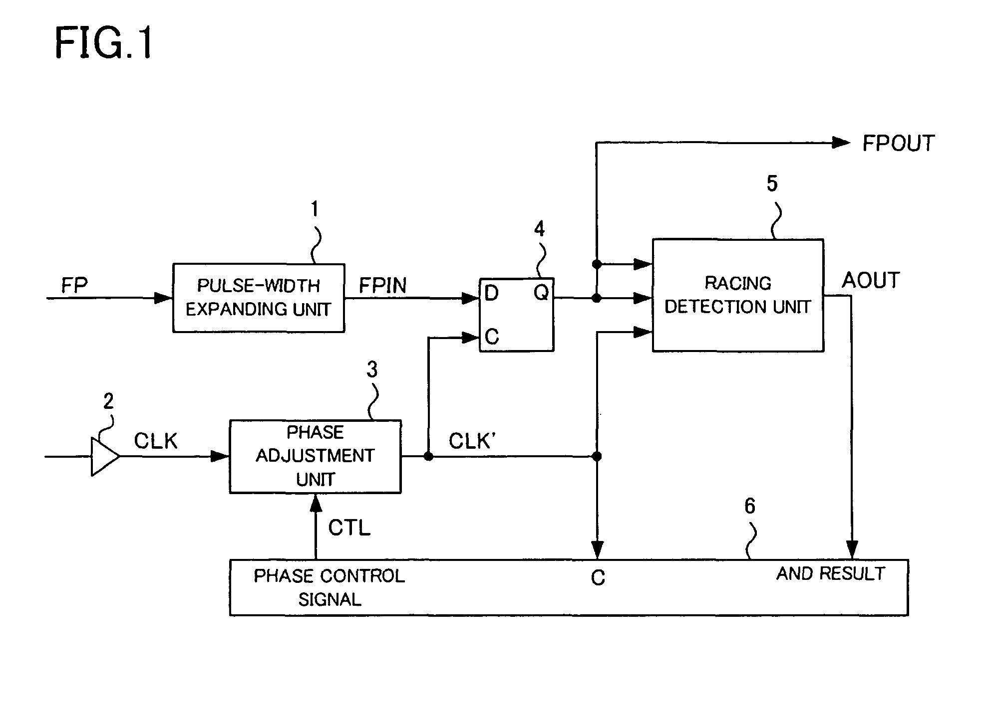
[0036]Hereinafter, embodiments of the present invention will be explained with reference to drawings. FIG. 1 is a block diagram showing a configuration of a frame pulse signal latch circuit according to a first embodiment of the present invention.
[0037]The frame pulse signal latch circuit of the present embodiment has a pulse-width expanding unit 1, a buffer 2, a phase adjustment unit 3, a flip-flop 4, a racing detection unit 5, and a control unit 6.
[0038]The pulse-width expanding unit 1 receives an input frame pulse signal FP, which has a pulse width of an m (m is a positive integer)-clock cycle, from a transmitting side and outputs a frame pulse signal FPIN which is obtained by extending the pulse width of the frame pulse signal FP to be longer than the m-clock cycle.
[0039]The buffer 2 receives clocks from the transmitting side.
[0040]The phase adjustment unit 3 generates output clocks CLK′, which are obtained by adjusting the phase of input clocks CLK based on a directed phase adj...
second embodiment
[0055]Next, a second embodiment of the present invention will be explained. FIG. 3 is a block diagram showing a configuration of a frame pulse signal latch circuit according to the second embodiment of the present invention. The present embodiment explains the first embodiment in more detail. In the present embodiment, the pulse width of the frame pulse signal FP is a one-clock cycle.
[0056]The frame pulse signal latch circuit of the present embodiment has buffers 10 and 11, a PLL circuit 12, a flip-flop 13, a flip-flop 14, an AND circuit 15, and a control circuit 16.
[0057]The buffer 10 functions as the pulse-width expanding unit, which receives the frame pulse signal FP from the transmitting side. The buffer 11 receives clocks from the transmitting side.
[0058]The PLL circuit 12 functions as the phase adjustment unit which adjusts the phase of the clocks CLK output from the buffer 11 and outputs the clocks CLK′ which has been phase-adjusted.
[0059]The flip-flop 13 functions as the lat...
third embodiment
[0081]Next, a third embodiment of the present invention will be explained. FIG. 8 is a block diagram showing a configuration of a frame pulse signal latch circuit according to the third embodiment of the present invention. Note that constituents similar to the constituents shown in FIG. 3 are denoted by the same reference numerals. In the present embodiment, the pulse width of the frame pulse signal FP is a two-clock cycle.
[0082]The frame pulse signal latch circuit of the present embodiment has the buffers 10 and 11, the PLL circuit 12, the flip-flops 13, 14, and 17, an AND circuit 15a, and the control circuit 16.
[0083]The buffer 10 receives the frame pulse signal FP from the transmitting side. The buffer 11 receives clocks from the transmitting side.
[0084]The PLL circuit 12 adjusts the phase of the clocks CLK, which is output from the buffer 11, and outputs the adjusted clocks CLK′.
[0085]The flip-flop 13 latches the frame pulse signal FPIN, which is output from the buffer 10, in sy...
PUM
 Abstract
Description
Claims
Application Information
 - R&D
- Intellectual Property
- Life Sciences
- Materials
- Tech Scout
- Unparalleled Data Quality
- Higher Quality Content
- 60% Fewer Hallucinations
Browse by: Latest US Patents, China's latest patents, Technical Efficacy Thesaurus, Application Domain, Technology Topic, Popular Technical Reports.
© 2025 PatSnap. All rights reserved.Legal|Privacy policy|Modern Slavery Act Transparency Statement|Sitemap|About US| Contact US: help@patsnap.com


