
Memory card and method for fabricating the same

a memory card and manufacturing method technology, applied in the field of memory cards, can solve the problems of increasing cost, complicating the manufacturing process, and inability to meet economic efficiency, so as to reduce the space for filling packaging materials, simplify the manufacturing process, and prevent leakage of packaging materials

Active Publication Date: 2010-09-14
UTAC HEADQUARTERS PTE LTD
View PDF14 Cites 20 Cited by
  • Summary
  • Abstract
  • Description
  • Claims
  • Application Information

AI Technical Summary

Benefits of technology

[0014]Another objective of the present invention is to provide a memory card and method for fabricating the same so as to simplify the fabricating process.
[0015]Another objective of the present invention is to provide a memory card and method for fabricating the same so as to shorten the fabricating time.
[0016]A further objective of the present invention is to provide a memory card and method for fabricating the same so as to improve the fabricating yield and reduce the fabricating cost.
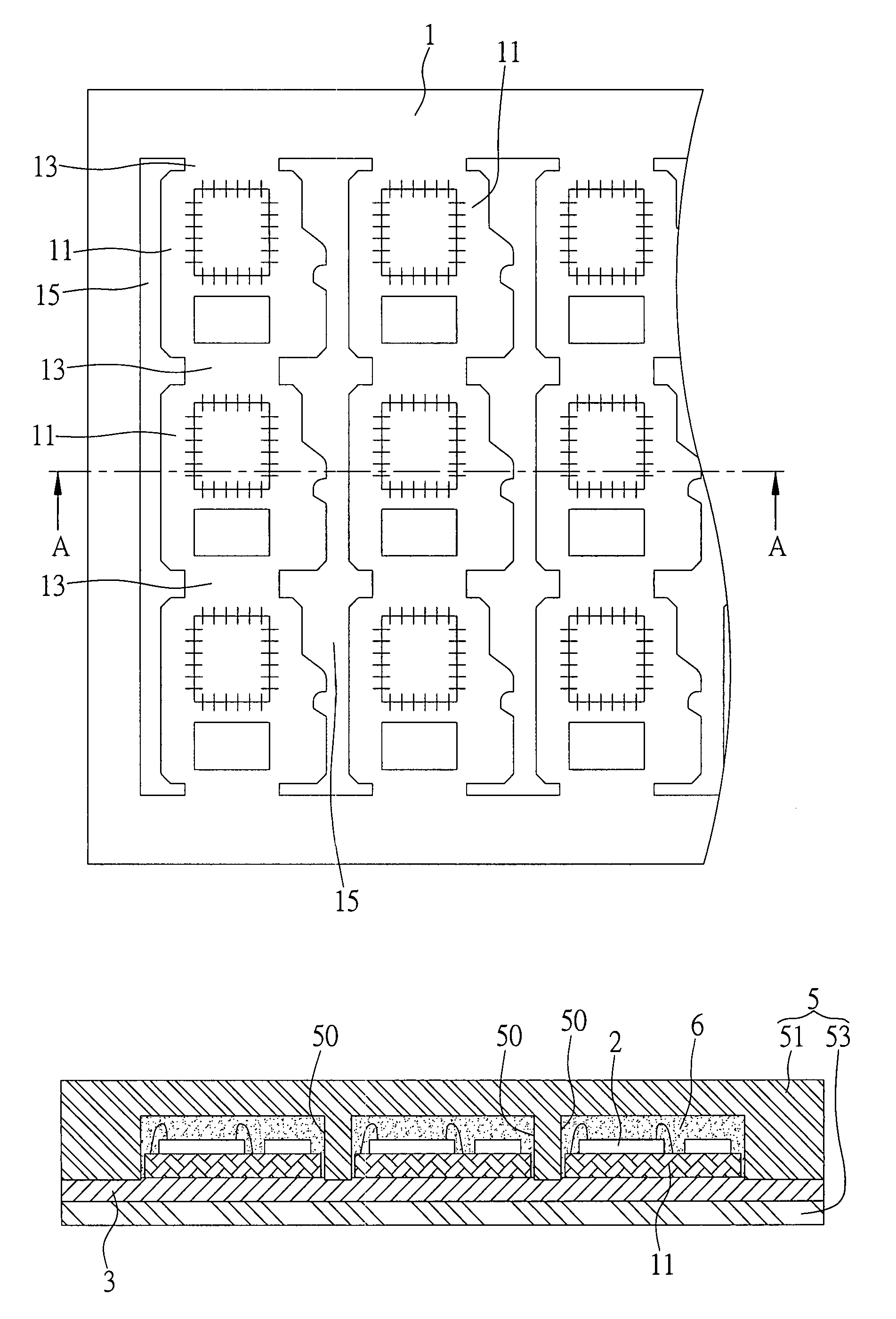
[0023]The mold comprises a lower mold abutting against the thin film and an upper mold covering the circuit board and the thin film, by defining the mold cavities through the upper mold and the thin film, space for filling of the packaging material is limited, thereby preventing leakage of the packaging material
[0024]Therefore, according to the memory card and method for fabricating the same of the present invention, only by cutting away the connecting portions, the circuit board units can be separated from each other so as to obtain memory cards of card type packages of irregular shape such as Micro-SD, MMC-Micro or Memory Stick Micro (M2). Compared with the prior art that needs to cut encapsulant along an irregular cutting path around each circuit board unit, the present invention eliminates the need to perform a shape cutting process by using such as a grinding tool, water jet or laser, thereby simplifying the fabricating process and shortening the fabricating time. By avoiding the use of the tools such as a grinding tool, water jet or laser as in the prior art, the present invention reduces the equipment cost, improves the fabricating yield and reduces the fabricating cost. Meanwhile, the present invention avoids chip-out or cracking of the encapsulant caused by use of water jet or laser as in the prior art. Thus, the memory card and method for fabricating the same according to the present invention overcome the drawbacks of the prior art.

Problems solved by technology

However, the memory card can easily break or be damaged from the bonding position or tiny spacing can appear at the bonding position after many times the memory card is inserted into and taken out from an electronic product over a long period of time.
However, the need of the housing and adhering the housing to the package increase cost and complicate the fabricating process, which cannot meet economic efficiency.
However, the above-described grinding wheel cutter can only form straight line cutting path and accordingly cannot meet demand of card type packages in irregular shape such as Micro-SD, MMC-Micro and M2.
However, the technique can only be used to fabricate MMC type memory cards and cannot be used to fabricate memory cards of irregular shape such as MMC-Micro and Micro-SD.
But the water jet process needs high cost.
Also, since an abrasive material of fine sand needs to be added to the water column of the water jet, the powder and the slag generated by the fine sand pollute the environment.
Also, because the abrasive material must be discarded after one time use and cannot be recycled, the fabricating cost is relatively high.
Further, as the cutting width and cutting path of the water jet are limited by pressure of the water jet and size of particles of the abrasive material, during cutting irregular packages, the cutting path can be unstable, which can adversely affect the fabricating yield.
Further, the nozzle of the water jet may sometimes be blocked by the abrasive material, which relatively increases instability of the process.
Moreover, as the cutting surface is often washed by the fine sand, it can become uneven.
However, the laser cut can lead to burning of the encapsulant and periphery of the circuit board, and result in an uneven cutting surface.
Meanwhile, the laser cut can cause such problems as burr cuts and powder pollution.
Also, the laser cutting cost (such as laser cutting equipment and lamp cost) is too high and cannot meet economic efficiency.
Moreover, both the water jet and laser cutting can result in chip-out or cracking of the encapsulant when cutting from the upper side of encapsulant downward using fine sand or energized beam, thereby adversely affecting the shape and quality of the memory card packages.

Method used


Image

  • Memory card and method for fabricating the same
  • Memory card and method for fabricating the same
  • Memory card and method for fabricating the same

Examples


Embodiment Construction

[0027]The following illustrative embodiments are provided to illustrate the disclosure of the present invention, these and other advantages and effects can be apparent to those skilled in the art after reading the disclosure of this specification. The present invention can also be performed or applied by other different embodiments. The details of the specification may be on the basis of different points and applications, and numerous modifications and variations can be made without departing from the spirit of the present invention.

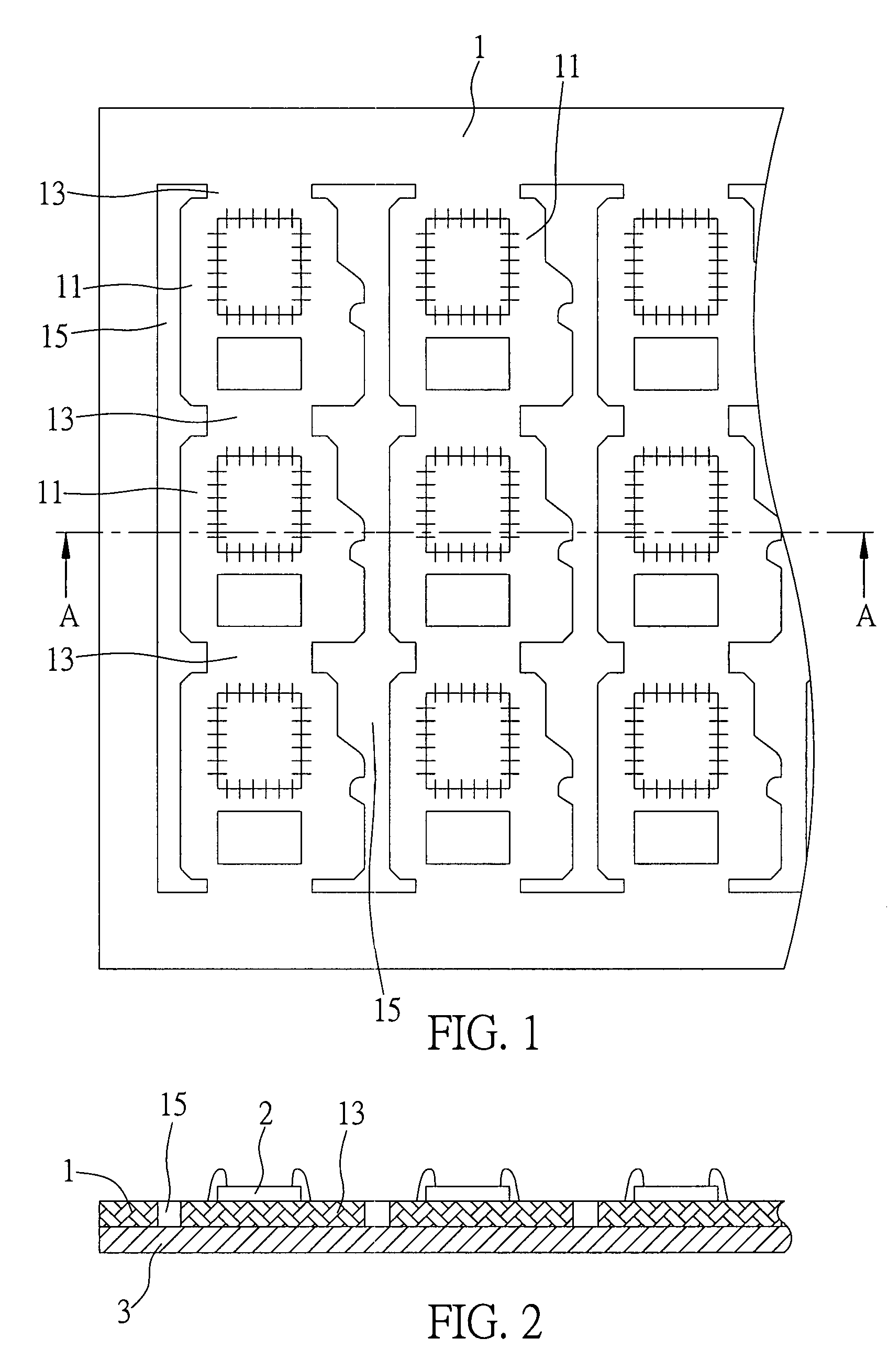
[0028]FIGS. 1 to 5B are diagrams showing a memory card and a method for fabricating the same according to the present invention.

[0029]As shown in FIG. 1, a circuit board 1 is provided, which comprises a plurality of spacing arranged circuit board units 11. Each circuit board unit 11 has a predefined shape of a memory card and is connected to the circuit board 1 through a connecting portion 13. At least a chip 2 is disposed on and electrically connected t...


PUM

PropertyMeasurementUnit
diameteraaaaaaaaaa
shapeaaaaaaaaaa
sizeaaaaaaaaaa

Abstract

A memory card and method for fabricating the same are disclosed, which includes mounting and electrically connecting at least a chip to a circuit board unit having a predefined shape of a memory card; attaching a thin film to the surface of the circuit board unit opposed to the surface with the chip mounted thereon; covering the circuit board unit and the thin film by a mold so as to form a mold cavity having same shape as the circuit board unit but bigger size; filling a packaging material in the mold cavity so as to form an encapsulant encapsulating the chip and outer sides of the circuit board unit, thus integrally forming a memory card having the predefined shape. The present invention eliminates the need to perform a shape cutting process by using water jet or laser as in the prior art, thus reducing the fabricating cost and improving the fabricating yield.

Description

BACKGROUND OF THE INVENTION[0001]1. Field of the Invention[0002]The present invention relates generally to a semiconductor packaging technique, and more particularly to a memory card and method for fabricating the same.[0003]2. Description of Related Art[0004]With the increasing development of digital products such as cameras, mobile phones, PDAs (Personal Digital Assistants), video and audio players, demands for flash memory cards are increasing. The flash memory cards are generally categorized into CF (Compact Flash) cards, SMCs (Smart Media Cards), MMCs (Multi Media Cards), SD (Secure Digital) cards, MS (Memory Stick) cards and so on. While the storage capacity of the memory cards keeps growing, structure of the memory cards is continuously improved so as to prevent easy breaking of the memory cards and meanwhile allow the memory cards to obtain a desired waterproof effect.[0005]A conventional memory card generally comprises two sheets with a circuit board disposed therebetween. ...

Claims


Application Information

Patent Timeline
Patent Type & Authority Patents(United States)
IPC IPC(8): H01L21/48
CPCH01L21/561H01L23/3121H01L24/97H05K3/284H01L21/568Y10T29/49002H01L2224/48091H01L2224/48227H01L2224/49175H01L2224/97H01L2924/01082H05K1/117H05K3/0052H05K2201/0909H05K2201/10159H05K2203/0156H05K2203/1316H01L24/49H01L2924/01033H01L2924/01005H01L24/48H01L2224/85H01L2924/00014H01L2924/00H01L2924/181H01L2924/00012H01L2224/45099H01L2224/45015H01L2924/207G06F1/00G06K19/07G06K19/077
Inventor TSAI, MING-SUNGHSU, HSIEH-WEI
Owner UTAC HEADQUARTERS PTE LTD
Learn More