Multiple electronic component containing substrate

a technology of electronic components and substrates, applied in the direction of printed circuit non-printed electric components, semiconductor devices, semiconductor/solid-state device details, etc., can solve the problems of increasing the production cost of electronic components contained substrates, increasing the b>400/b>, and increasing the length of bonding wires, so as to reduce the planar dimension (a plane area) and the effect of low cos

Active Publication Date: 2010-08-10
SHINKO ELECTRIC IND CO LTD
View PDF22 Cites 21 Cited by
  • Summary
  • Abstract
  • Description
  • Claims
  • Application Information

AI Technical Summary

Benefits of technology

[0009]Exemplary embodiments of the present invention provide an electronic component contained substrate containing a plurality of electronic components in a stacked state that can reduce a planar dimension (a plane area) considerably and can be manufactured at a low cost.
[0016]The second electronic component may be mounted such that a surface to which the wire bonding is applied is positioned within a thickness of the other wiring substrate. Thus, a height position of the wire-bonding surface of the second electronic component can be lowered with respect to the connection pad of the other wiring substrate. Therefore, in wire-bonding the second electronic component and the other wiring substrate, a top height of a wire loop formed by the bonding wire can be lowered. As a result, a thickness dimension of the electronic component contained substrate can be reduced.
[0017]Also, the first electronic component may be coated with the sealing resin, and the second electronic component may be mounted on a surface of the sealing resin. Therefore, the manufacture of the electronic component contained substrate can be facilitated, and thus the inexpensive electronic component contained substrate can be provided.
[0018]Also, the second electronic component may be adhered directly to the first electronic component. Therefore, a space between one wiring substrate and the other wiring substrate, the first and second electronic components, and the bonding wires can be sealed all together by the resin. As a result, the number of times of the resin sealing steps can be reduced.
[0020]According to the electronic component contained substrate according to the present invention, electrode positions of the second electronic component being connected to the other wiring substrate by the wire bonding can be brought closer to the connection pads of the other wiring substrate. Therefore, a length of the bonding wire can be reduced considerably and also the electronic component contained substrate with high electrical reliability can be provided at a low cost.

Problems solved by technology

As a result, such a problem exists that a length of the bonding wire 260 becomes longer.
As a result, such a problem also exists that a production cost of the electronic component contained substrate adds up.
In this manner, when the electronic components such as the semiconductor elements, or the like are mounted in a plural-stage stacked fashion, such problems arise that a planar dimension (a plane area) of an electronic component contained substrate 400 is increased and a production cost is increased.

Method used


Image

  • Multiple electronic component containing substrate
  • Multiple electronic component containing substrate
  • Multiple electronic component containing substrate

Examples


first embodiment

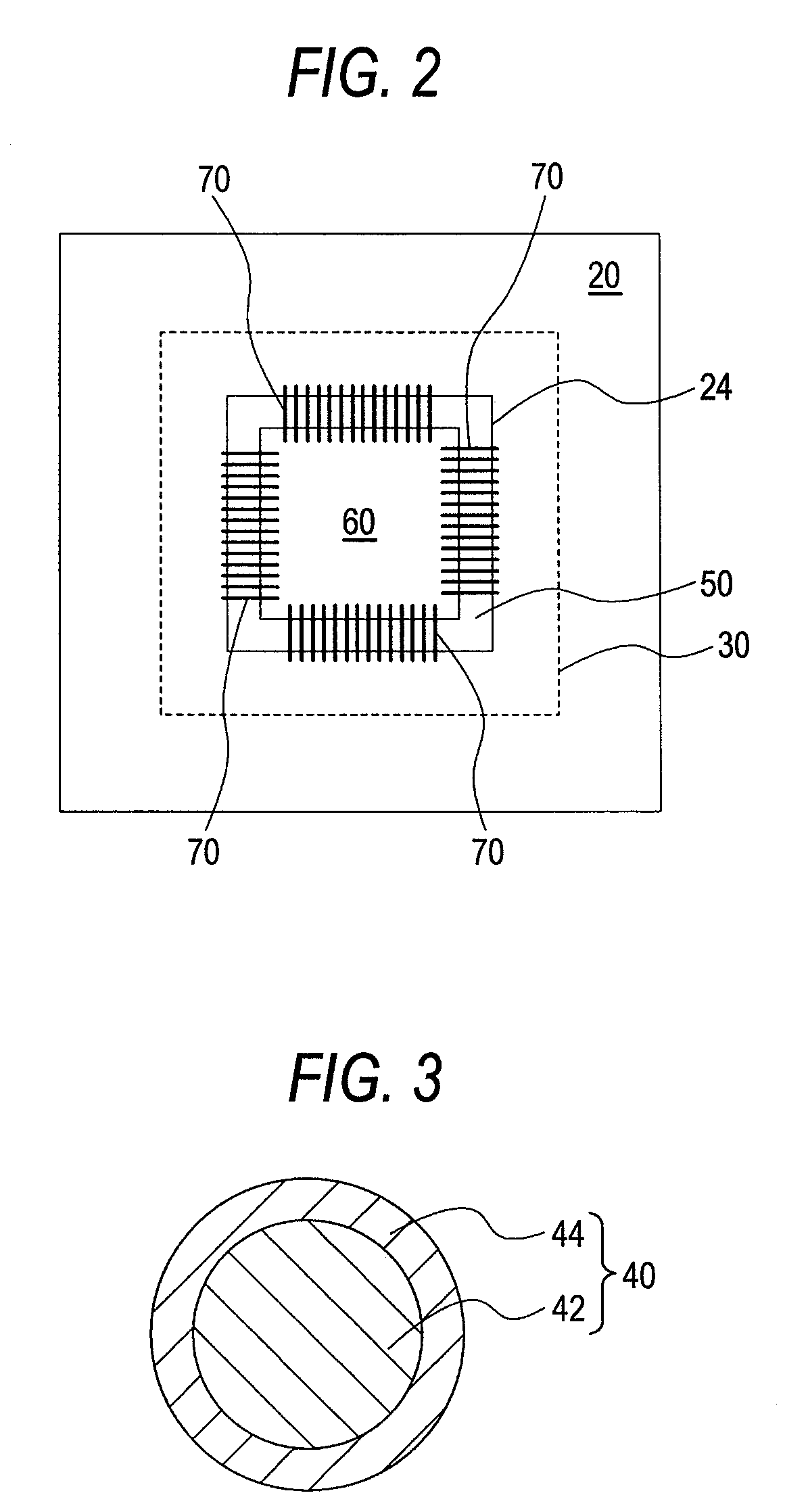
[0033]A first embodiment of an electronic component contained substrate according to the present invention will be explained with reference to the drawings hereinafter. FIG. 1 is a cross sectional view of an electronic component contained substrate in a first embodiment of the present invention. FIG. 2 is a plan view of an opening portion and its neighboring area in the electronic component contained substrate shown in FIG. 1. FIG. 3 is a sectional view showing a structure of a solder ball used in the present embodiment.

[0034]In the present embodiment, an electronic component contained substrate 100 is constructed such that a first semiconductor element 30 as a first electronic component is mounted between a pair of wiring substrates (a wiring substrate 10 on a lower layer side and a wiring substrate 20 on an upper layer side) and also a second semiconductor element 60 as a second electronic component is mounted on the first semiconductor element 30. The first semiconductor element ...

second embodiment

[0060]FIG. 10 is a cross sectional view showing a structure of an electronic component contained substrate in a second embodiment of the present invention. Concretely, the electronic component contained substrate 100 is constructed by mounting the second semiconductor element 60 directly on the back surface side of the first semiconductor element 30.

[0061]In the present embodiment, in the step applied just before the sealing resin 50 is filled into a space between the wiring substrate 10 and the wiring substrate 20 (i.e., in the state that the wiring substrate 20 is joined to the wiring substrate 10 via the solder balls), if the wiring substrate 20 has a mechanical strength enough to withstand the wire bonding operation between the second semiconductor element 60 and the wiring substrate 20, the wiring substrate 10, the wiring substrate 20, and the second semiconductor element 60 can be sealed all together with the sealing resin 50 after the second semiconductor element 60 and the w...


PUM


Abstract

In an electronic component contained substrate in which electronic components are mounted between a pair of wiring substrates in a plural-stage stacked fashion, one wiring substrate and other wiring substrate are connected electrically mutually via solder balls, a first electronic component is mounted on one wiring substrate and then a second electronic component is mounted on the first electronic component, an opening portion for containing the second electronic component therein is provided in the other wiring substrate, the second electronic component is contained and mounted in the opening portion and is connected electrically to the other wiring substrate by a wire bonding, and a space between the pair of wiring substrates is sealed with a sealing resin.

Description

[0001]This application claims priority from Japanese Patent Application No. 2006-348755, filed Dec. 26, 2006, in the Japanese Patent Office. The Japanese Patent Application No. 2006-348755 is incorporated by reference in its entirety.TECHNICAL FIELD[0002]The present disclosure relates to an electronic component contained substrate and, more particularly, an electronic component contained substrate in which a plurality of electronic components are stacked and mounted between a pair of wiring substrates.RELATED ART[0003]As the electronic component contained substrate that contains the electronic component to put it between two sheets of wiring substrates, the product in a mode shown in FIG. 11 has been proposed (see the paragraph 0073 of Patent Literature 1 (Japanese Patent Unexamined Publication No. 2005-310984), for example). This product is formed by stacking two semiconductor devices 300A, 300B. The semiconductor devices 300A, 300B are connected electrically by joining electrodes ...

Claims


Application Information

Patent Timeline
Patent Type & Authority Patents(United States)
IPC IPC(8): H01L23/02H01L23/34H01L23/48H01L23/52H01L29/40
CPCH01L21/563H01L23/5385H01L25/0657H01L2224/48091H01L2924/00014H01L2224/16225H01L2224/48227H01L2224/73203H01L2224/73265H01L2225/0651H01L2225/06517H01L2225/06527H01L2924/01078H01L2924/01079H01L2924/15153H01L2924/15311H01L2924/19041H01L24/48H01L2224/32225H01L2224/73204H01L2924/00H01L2224/45144H01L2224/32145H01L2924/00012H01L2224/73253H01L24/45H01L24/73H01L2924/181H01L2224/05599H05K1/18
Inventor INOUE, AKINOBU
Owner SHINKO ELECTRIC IND CO LTD
Why Eureka
Try Eureka