Nonvolatile memory device
a memory device and non-volatile technology, applied in semiconductor devices, digital storage, instruments, etc., can solve the problems of long time required for rewriting and the restriction of attaining higher speed, and achieve the effect of reducing resistance, high reliability, and suppressing the occurrence of corruptive routines
- Summary
- Abstract
- Description
- Claims
- Application Information
AI Technical Summary
Benefits of technology
Problems solved by technology
Method used
Image
Examples
embodiment 1
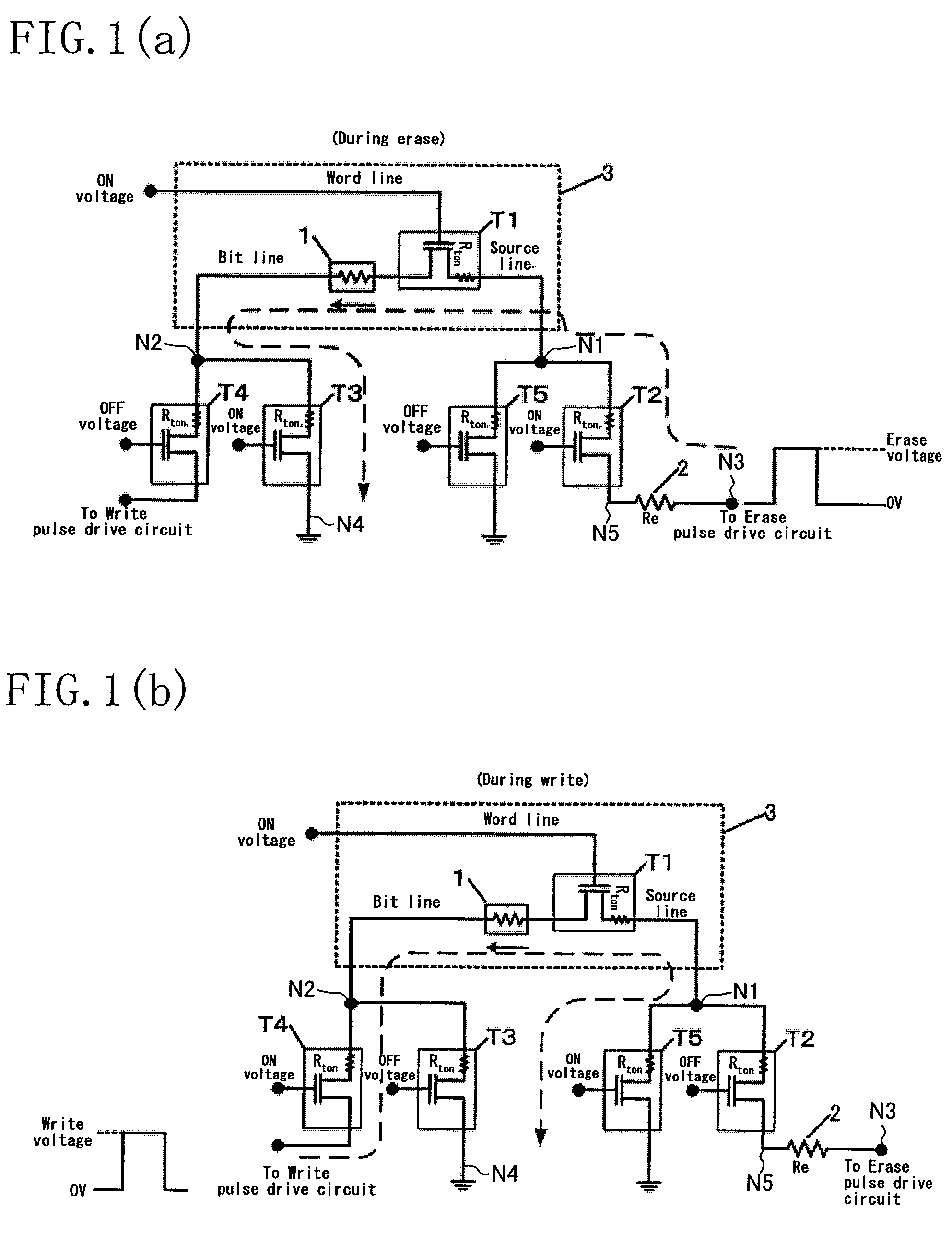
[0049]FIG. 1 shows a configuration of a memory cell of an inventive device together with configurations of drive circuits in the states of applying an erase pulse and a write pulse to the memory cell. Note that the erase pulse as used herein is defined as a pulse that changes a variable resistance element from high resistance to low resistance, in which the pulse width and the voltage amplitude are predetermined values. Note also that the write pulse as used herein is defined as a pulse that, in reverse to the erase pulse, changes a variable resistance element from low resistance to high resistance, in which, similarly to the above, the pulse width and the voltage amplitude are predetermined values corresponding to the element.
[0050]As shown in FIGS. 1(a) and 1(b), the nonvolatile memory device of this embodiment includes a memory cell 3, selection transistors T2 to T5 and an erase pulse limiting fixed resistance 2.
[0051]The memory cell 3 includes a variable resistance element 1 and...
embodiment 2
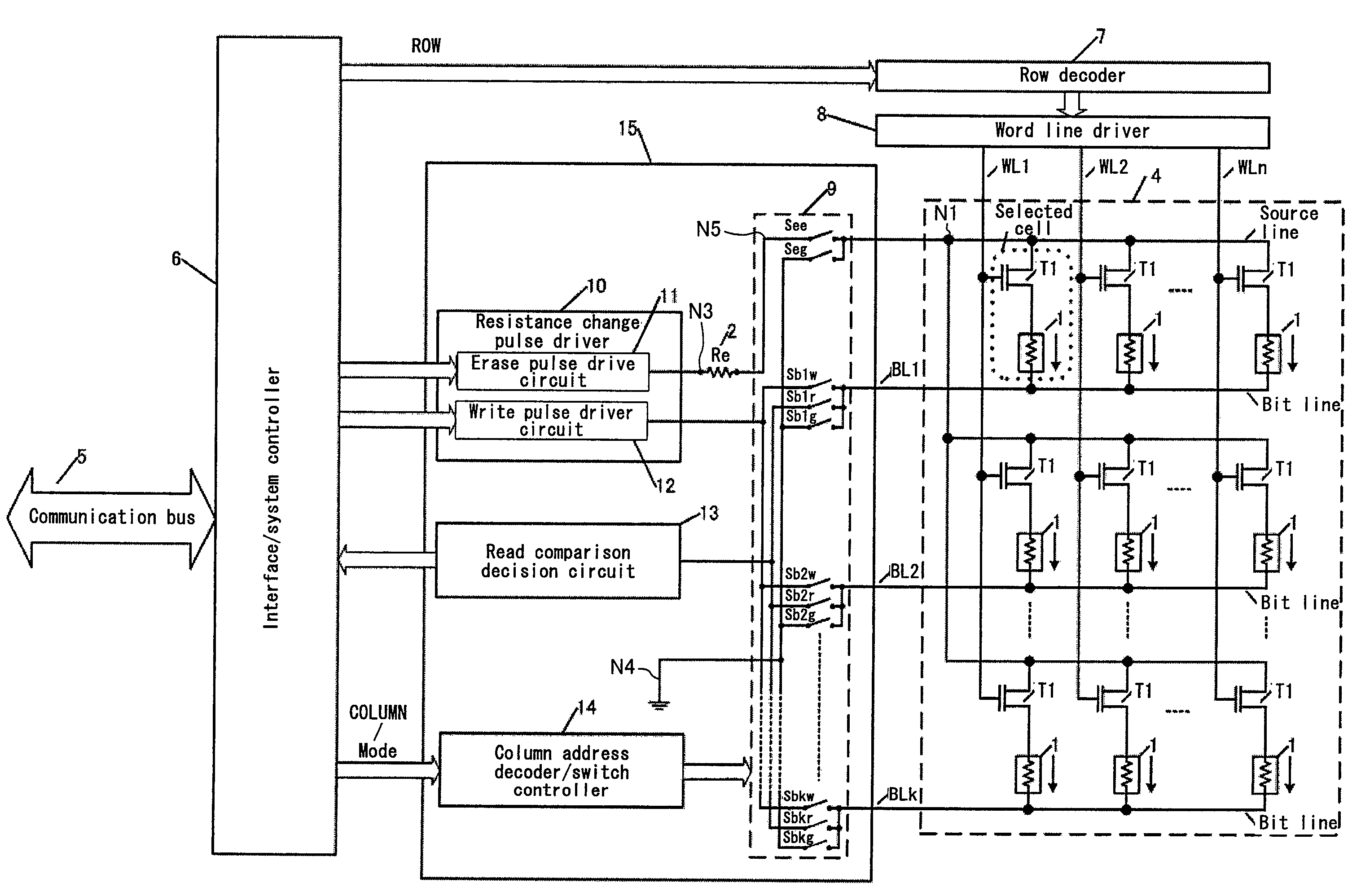
[0064]The inventive device of Embodiment 2 will be described with reference to the relevant drawing. FIG. 7 is a block diagram of a nonvolatile memory device of this embodiment. In FIG. 7, a memory cell array 4 includes a plurality of memory cells arranged in a matrix. Each of the memory cells is the memory cell described in Embodiment 1. The same reference numerals as those in FIG. 1 are therefore the same in operation and thus description thereof is omitted here. In the memory cell array 4, the gates of transistors T1 (first selection switch elements) in each row are short-circuited (commonly connected to the corresponding word line WL1, WL2, . . . , WLn). Each bit line for cells in each column is also short-circuited (terminals of variable resistance elements 1 in each column are commonly connected to the corresponding bit line BL1, BL2, . . . , BLk via second nodes). Moreover, all source lines for all cells are short-circuited (terminals of transistors T1 of the cells are common...
embodiment 3
[0070]The inventive device of Embodiment 3 will be described with reference to the relevant drawing. FIG. 8 is a block diagram of a nonvolatile memory device of Embodiment 3. In FIG. 8, the same reference numerals as those in FIG. 7 are the same in function and thus description thereof is omitted here. The point different from FIG. 7 is that an erase pulse limiting variable resistance 16 is provided in place of the erase pulse limiting fixed resistance 2. The erase pulse limiting variable resistance 16 can change the resistance value in stages under an instruction from the system controller 6. The internal circuit configuration of the erase pulse limiting variable resistance 16 is not specifically shown, but can be implemented by configuring a resistance array composed of predetermined fixed resistances connected in series and selecting an appropriate number of resistances using transistor switches.
[0071]With the configuration of this embodiment, the following advantage can be obtai...
PUM
 Abstract
Description
Claims
Application Information
 - R&D
- Intellectual Property
- Life Sciences
- Materials
- Tech Scout
- Unparalleled Data Quality
- Higher Quality Content
- 60% Fewer Hallucinations
Browse by: Latest US Patents, China's latest patents, Technical Efficacy Thesaurus, Application Domain, Technology Topic, Popular Technical Reports.
© 2025 PatSnap. All rights reserved.Legal|Privacy policy|Modern Slavery Act Transparency Statement|Sitemap|About US| Contact US: help@patsnap.com


