Eureka AIR delivers breakthrough ideas for toughest innovation challenges, trusted by R&D personnel around the world.

Light source apparatus and display apparatus and white resist layer

a technology of light source apparatus and resist layer, which is applied in the direction of electrical apparatus, basic electric elements, semiconductor devices, etc., can solve the problems that the arrangement of light-emitting diodes that has been proposed so far is still insufficient to improve the efficiency at which light can be emitted from them, and achieves the reduction of power consumption of light source apparatus, the effect of maintaining sufficient intensity of emitted light and low energy

Inactive Publication Date: 2010-06-01
SONY CORP
View PDF21 Cites 20 Cited by
  • Summary
  • Abstract
  • Description
  • Claims
  • Application Information

AI Technical Summary

Benefits of technology

[0011]In order to solve the above-mentioned problems, the present invention provides a light source apparatus which can improve efficiency at which light is emitted from light-emitting diode chips and to provide a display apparatus including the light source apparatus.
[0027]Also, the number of the light-emitting devices can be reduced to make the display apparatus small-sized and to reduce component cost.

Problems solved by technology

However, the arrangements that have been proposed so far are still insufficient to improve efficiency at which light can be emitted from the light-emitting diode chips.

Method used


Image

  • Light source apparatus and display apparatus and white resist layer
  • Light source apparatus and display apparatus and white resist layer
  • Light source apparatus and display apparatus and white resist layer

Examples


examples

[0262]Subsequently, light source apparatuses were manufactured in practice and reflection spectral distributions were measured.

[0263]In the examples, the white resist layer 6 was formed on the substrate 1 and the electrodes 2, 3, the thickness of the white resist layer 6 was changed to 40 μm, 30 μm and 22.5 μm and then respective samples were manufactured.

[0264]In addition, samples without the white resist layer 6 were fabricated as comparative examples.

[0265]With respect to the respective samples, reflection spectral distributions on the electrodes (wirings) 2, 3 were measured. In the samples of the comparative examples, reflection spectral distributions on the outside of the electrodes (wirings) 2, 3 were also measured.

[0266]FIG. 27 shows measured results. Also, FIG. 27 shows reflection spectral distribution of Cu used for a wiring material, for reference.

[0267]From FIG. 27, it is to be understood that the respective examples in which the white resist layer 6 is formed on the elec...


PUM


Abstract

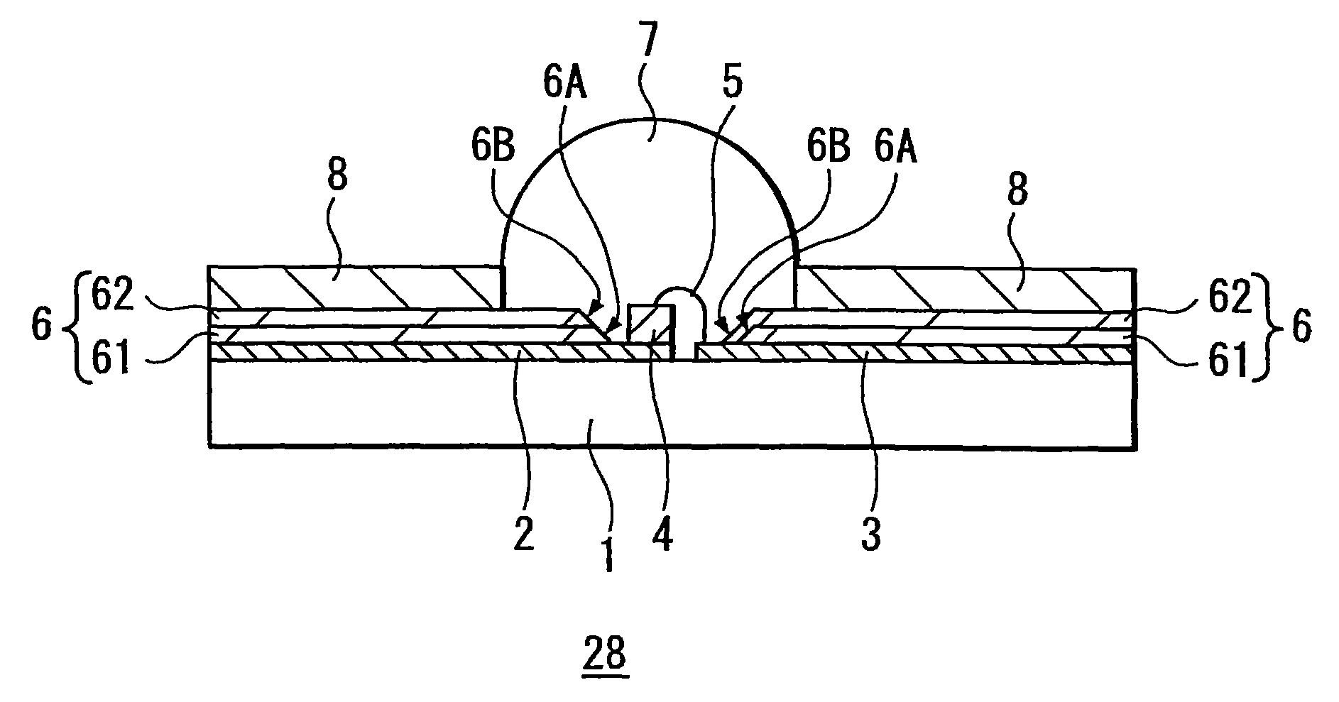
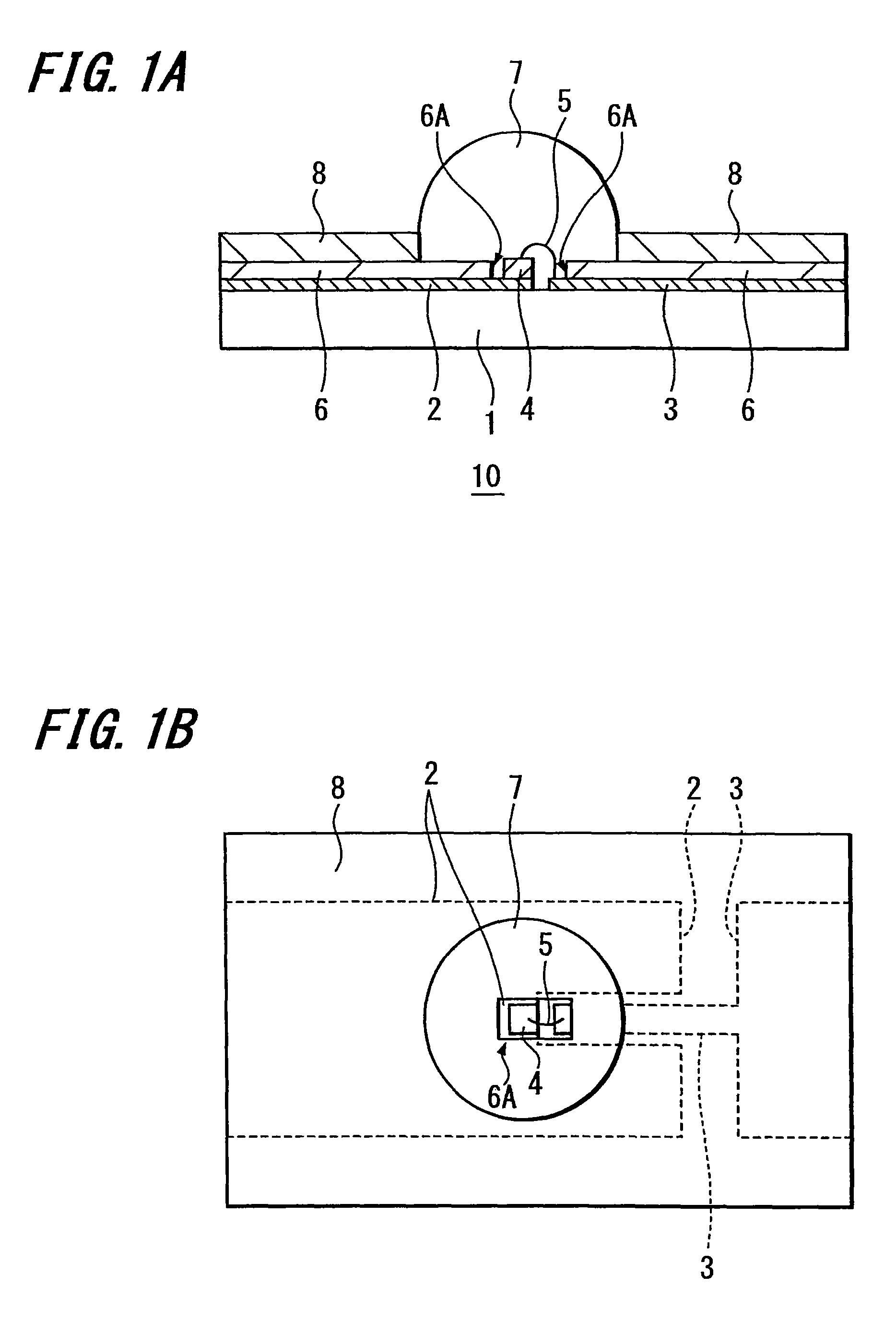
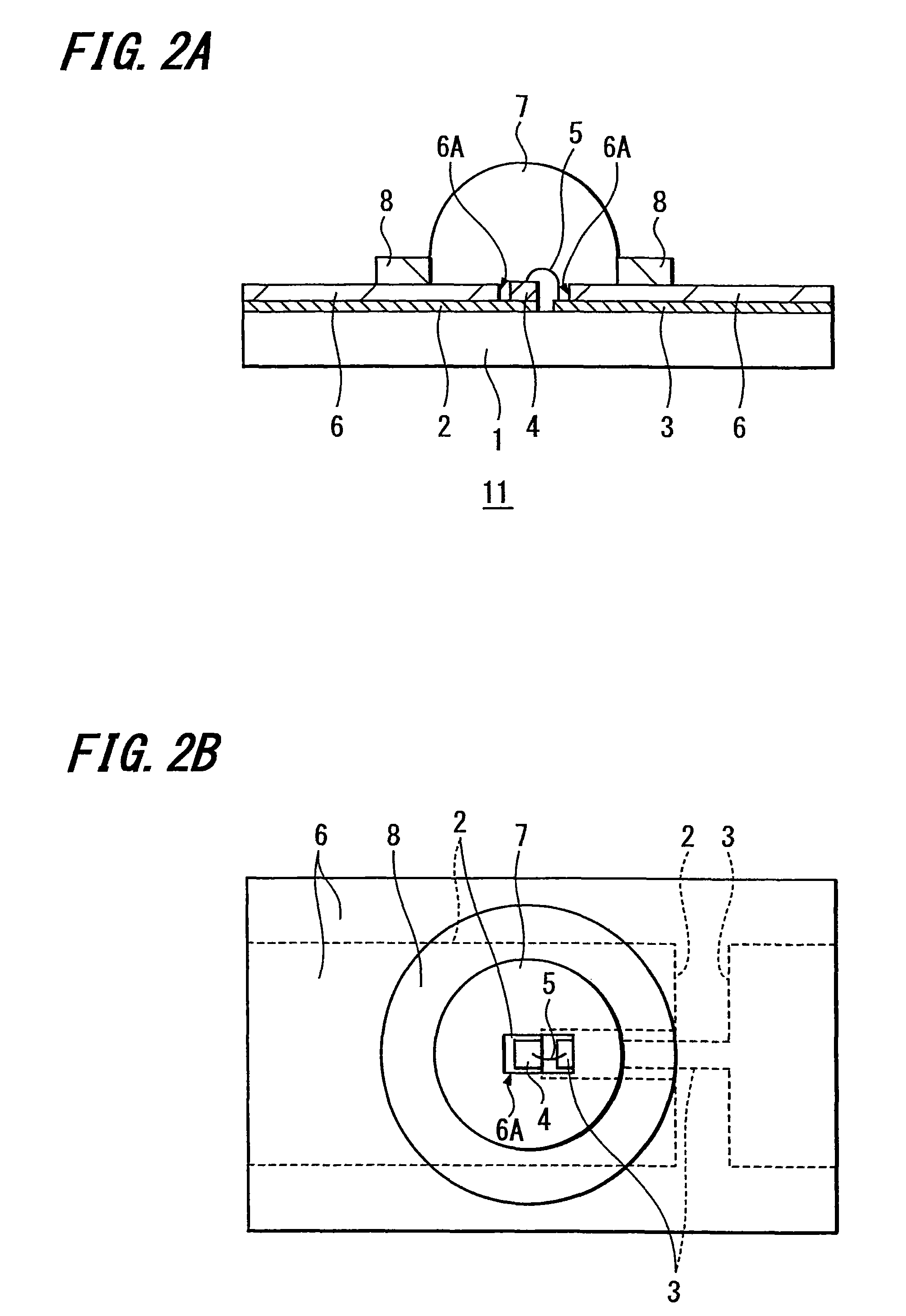
A light source apparatus is configured to generate light efficiently from a light-emitting device. The light source apparatus includes a substrate having a pair of electrodes, a light-emitting device and a transparent resin for sealing the light-emitting device. A white resist layer is formed on the substrate. The white resist layer is formed to cover apart of the electrodes. The white resist layer 6 includes an opening corresponding to the light-emitting device. A white member for controlling a shape of the transparent resin is formed on the white resist layer.

Description

TECHNICAL FIELD[0001]The present invention relates to a light source apparatus including a light-emitting device such as a light-emitting diode as a light source and the light source apparatus is suitable for use as the application to an illumination light source apparatus that can obtain a surface-light source of desired color (white or other colors). Also, the present invention relates to a display apparatus including a light source apparatus which illuminates a display unit from the back.BACKGROUND ART[0002]Since light-emitting diodes become able to generate high outputs in recent years, a white LED light source using a light-emitting diode (LED) is widely used to emit white light.[0003]In particular, such white LED light source may be applied to illumination apparatuses which are requested to generate high intensity, to projector apparatuses and backlights for large-scale liquid-crystal displays. For the uses, since the white LED light source has merits that it is mercury-free t...

Claims


Application Information

Patent Timeline
Patent Type & Authority Patents(United States)
IPC IPC(8): H01L27/15H01L29/267H01L31/12H01L33/00H01L33/54H01L33/56H01L33/60H01L33/62
CPCH01L33/60H01L33/52H01L33/54H01L2224/48091H01L2224/48227H01L2224/14H01L2924/181H01L2924/00014H01L2924/00011H01L2924/00012H01L2224/0401
Inventor FUJINO, TOYOMIFUJII, MASARUFUKASAWA, HIROYUKI
Owner SONY CORP
Why Eureka
Eureka Blog
Learn More