Semiconductor device

a technology of semiconductors and devices, applied in the field of semiconductor devices, can solve the problems of time waste in testing, difficult to reduce test time, and all refresh operations for refreshing the normal area, and achieve the effect of speeding up the refresh tes

Active Publication Date: 2010-05-18
LONGITUDE LICENSING LTD
View PDF6 Cites 8 Cited by
  • Summary
  • Abstract
  • Description
  • Claims
  • Application Information

AI Technical Summary

Benefits of technology

[0019]The refresh counter circuit in one mode of the present invention may rearrange address, when the redundancy area is tested, in such a manner that a row address of the redundancy area is reduced and placed on neighboring lower-order bits including the least significant bit (LSB) of a count output of the refresh counter circuit.
[0020]In accordance with the present invention, when a refresh test of a redundancy area is conducted, the configuration of a refresh counter circuit can be changed in such a manner that only enough addresses of a redundancy area are successively generated. As a result, the refresh test is speeded up.

Problems solved by technology

Consequently, in a case where all word lines of a redundancy area are refreshed, the refresh counter circuit must be made to perform a counting operation needlessly, with the result that time is wasted in testing.
This makes difficult to reduce test time.
That is, all refresh operations for refreshing of the normal area until the refresh counter circuit further counts up to a next count value corresponding to a word line in the redundancy area are wasteful.
As a result, it is very difficult to reduce test time at refreshing of a redundancy area, in a wafer test, etc.

Method used


Image

  • Semiconductor device
  • Semiconductor device
  • Semiconductor device

Examples


Embodiment Construction

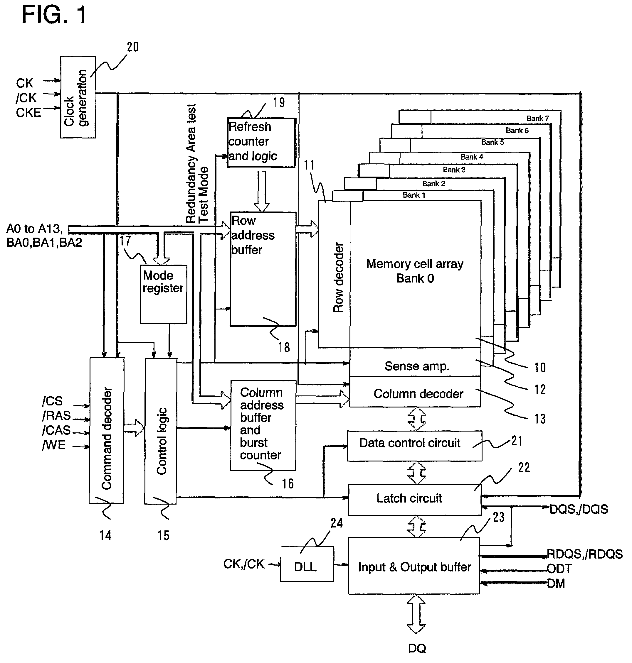
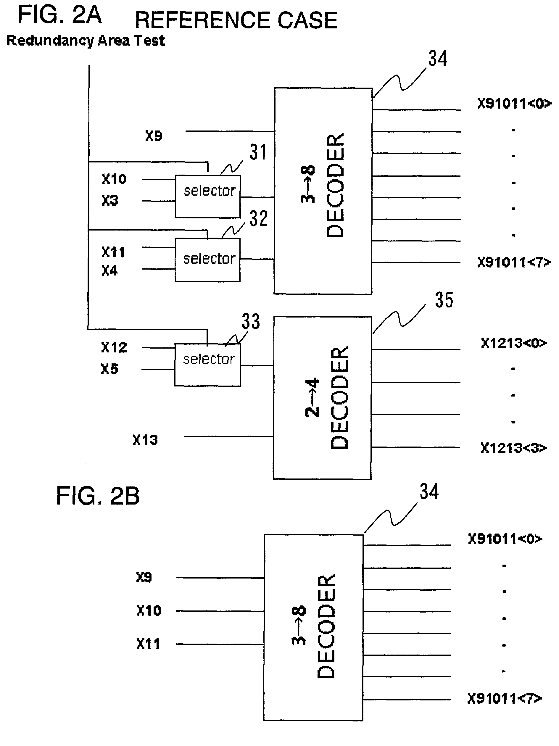
[0029]A preferred exemplary embodiment of the present invention will be described in detail with reference to the drawings. In the present invention, a cell array having a plurality of cells in need of refresh for data retention includes a redundancy area having a plurality of redundant cells for replacing faulty cells of a normal area within the cell array. When the redundancy area is tested, a refresh counter circuit which generates refresh addresses for the normal area, rearranges addresses in such a manner that an address of the redundancy area is placed on a lower-order bit side that includes the LSB of the counter.

[0030]When the test of the redundancy area is tested, refresh of word lines of the redundancy area is performed successively, based upon refresh addresses from the refresh counter circuit, owing to rearrangement of the addresses of the refresh counter circuit, and refresh of the normal area is not interposed between refreshes of word lines of the redundancy area.

[003...


PUM


Abstract

Disclosed is a semiconductor storage device in which a cell array including a plurality of cells in need of refresh for data retention includes the redundancy area, which has a plurality of redundant cells for replacing faulty cells of a normal area within the cell array. When the redundancy area is tested, a refresh counter circuit for generating and outputting refresh addresses rearranges the address in such a manner that a row address of the redundancy area is substantially reduced and placed on a lower-order bit side inclusive of the LSB of the counter.

Description

REFERENCE TO RELATED APPLICATION[0001]This application is based upon and claims the benefit of the priority of Japanese patent application No. 2007-189767, filed on Jul. 20, 2007, the disclosure of which is incorporated herein in its entirety by reference thereto.BACKGROUND OF THE INVENTION[0002]1. Field of the Invention[0003]This invention relates to a semiconductor device and, more particularly, to a semiconductor device having a memory that includes cells in need of refresh for data retention.[0004]2. Description of Related Art[0005]In a DRAM (Dynamic Random-Access Memory) provided with redundant cells for rescuing faulty cells, a faulty cell detected by for example a wafer test, is replaced with a redundant cell. More specifically, a word line of a faulty cell is replaced with a redundant word line in a redundancy area by fuse programming (fuse blowing) of a redundancy decoder circuit. As a result, when an X address (row address) to be accessed matches an X address of the faulty...

Claims


Application Information

Patent Timeline
Patent Type & Authority Patents(United States)
IPC IPC(8): G11C7/00
CPCG11C7/222G11C29/783G11C29/24G11C29/50016G11C11/406G11C7/22G11C11/401G11C11/4076
Inventor TANIMURA, NAOYASATO, TOMOHIKODONO, CHIAKI
Owner LONGITUDE LICENSING LTD
Why Eureka
Try Eureka