Digital signal transfer device
a digital signal and transfer circuit technology, applied in the direction of duplex signal operation, single pulse train generator, baseband system details, etc., can solve the problems of inability to transfer digital signals, inability to use photocouplers in high temperature environments of 100° c, and inability to achieve high-performance photocouplers, excellent performance, and high reliability
- Summary
- Abstract
- Description
- Claims
- Application Information
AI Technical Summary
Benefits of technology
Problems solved by technology
Method used
Image

Examples
first embodiment
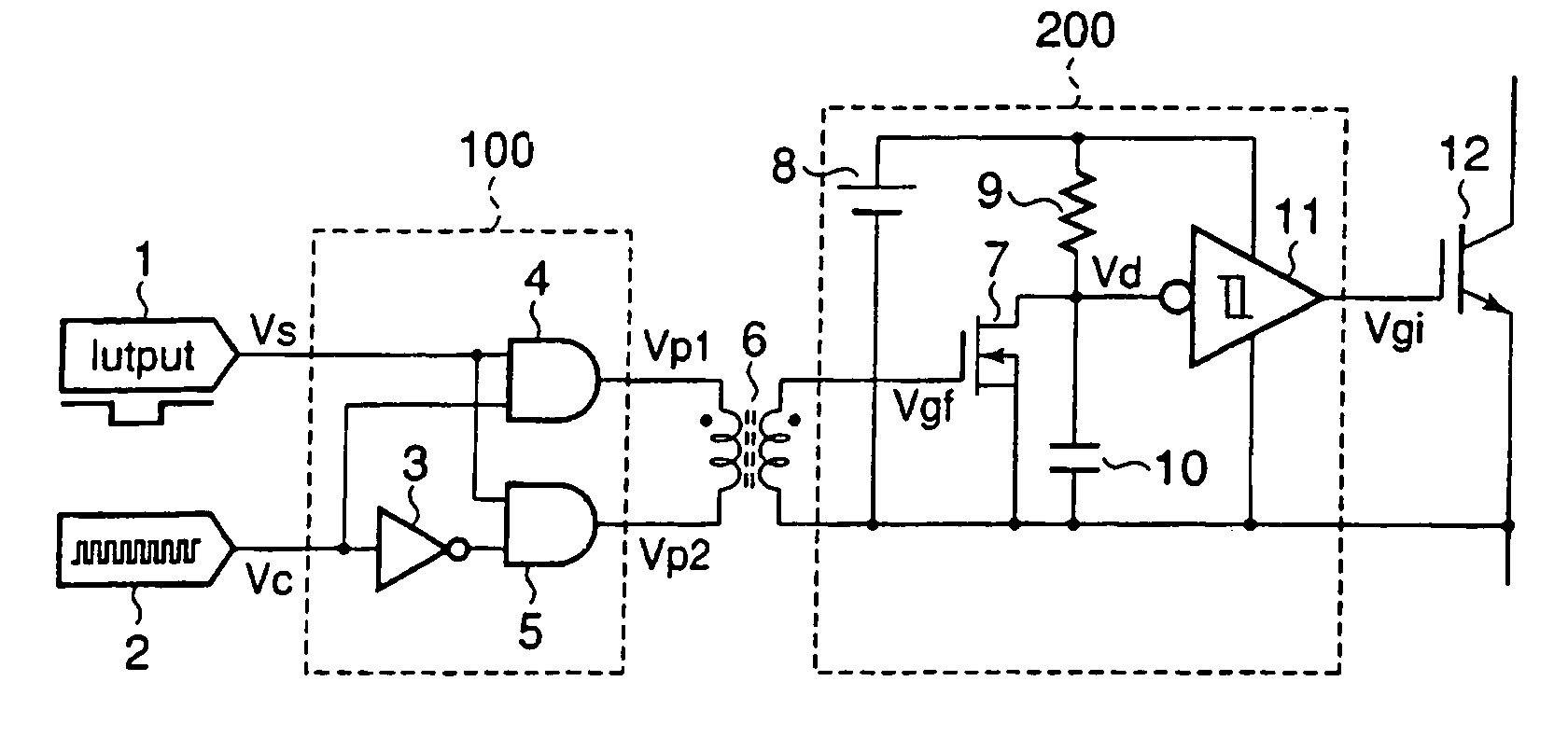
[0034]FIG. 1 is a view showing a detail of a gate drive circuit of for example an inverter employing a digital signal transfer circuit according to a first embodiment. FIG. 2A to FIG. 2G are timing charts given in explanation of the operation of this embodiment.
[0035]In general terms, this circuit comprises: a signal source 1 that outputs a digital signal (input signal wave) Vs, a carrier signal source 2 that generates a carrier signal Vc, a modulating section (input gate circuit) 100, a pulse transformer 6 constituting an isolating transfer section, and a demodulating section 200.
[0036]The signal source 1 outputs (see FIG. 2A) a digital signal (hereinbelow referred to as an on / off signal) Vs for drive control of an insulated gate transistor (hereinbelow referred to as an IGBT: insulated gate bipolar transistor) 12 constituting the driver of a gate drive circuit.
[0037]The carrier signal source 2 outputs (see FIG. 2B) a carrier signal Vc of a frequency that is sufficiently higher tha...
second embodiment
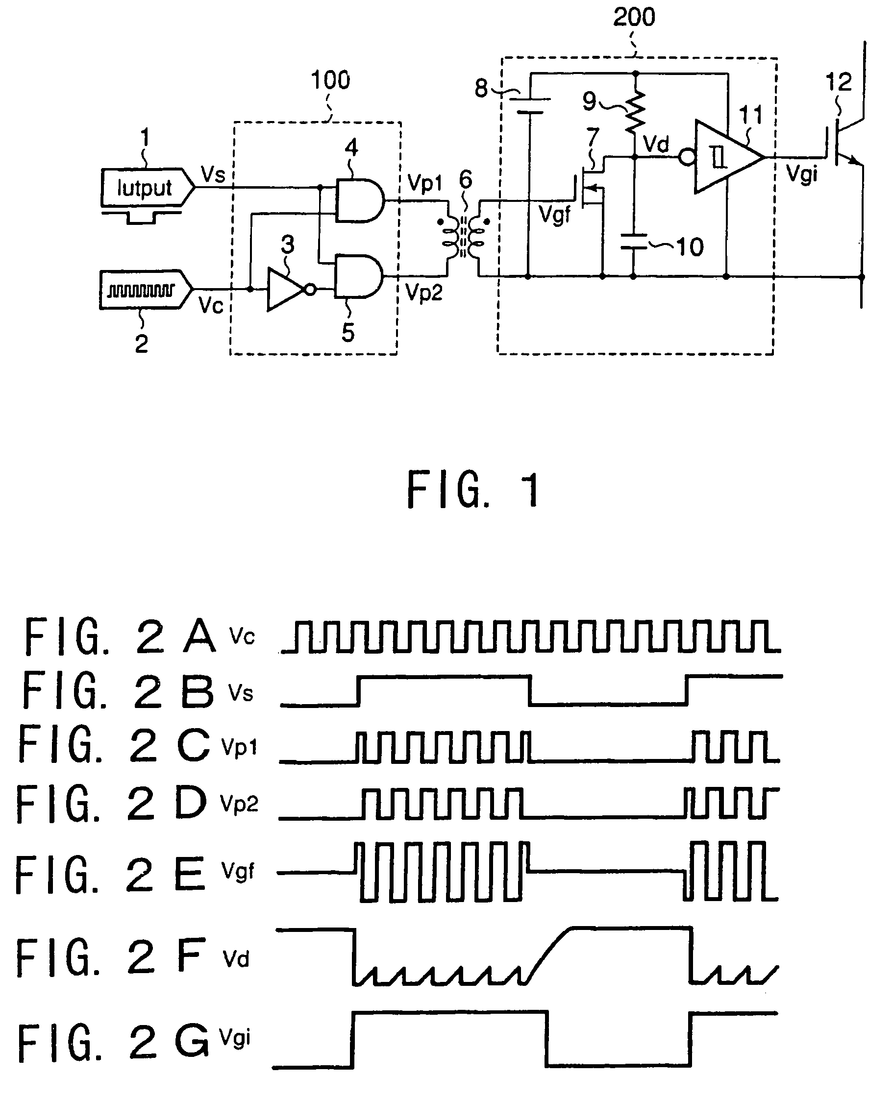
[0061]FIG. 3 and FIG. 4A to FIG. 4G are views given in explanation of a digital signal transfer circuit according to a second embodiment. The layout and beneficial effects of the digital signal transfer circuit according to the second embodiment will be described below with reference to FIG. 3 and FIG. 4A to FIG. 4G.
[0062]Layout and operation of this embodiment shown in FIG. 3 which are the same as in the case of the first embodiment shown in FIG. 1 are indicated by attaching the same reference symbols and detailed description is omitted.
[0063]The modulating section 100 of this embodiment comprises a first NAND circuit (hereinbelow called first NAND gate) 13 and second NAND circuit (hereinbelow called second NAND gate) 14.
[0064]The first input terminal of the first NAND gate 13 is connected with the output terminal of the signal source 1 and the second input terminal thereof is connected with the output terminal of the carrier signal source 2. The first NAND gate 13 outputs (see FIG...
third embodiment
[0074]FIG. 5 and FIG. 6A to FIG. 6G are views given in explanation of a digital signal transfer circuit according to a third embodiment. The layout and beneficial effects of the digital signal transfer circuit according to the third embodiment will be described below with reference to FIG. 5 and FIG. 6A to FIG. 6G.
[0075]Layout and operation of this embodiment shown in FIG. 5 which is the same as in the case of the first embodiment shown in FIG. 1 are indicated by attaching the same reference symbols and detailed description is omitted.
[0076]The modulating section 100 of this embodiment comprises a first OR gate circuit (hereinbelow called first OR gate) 15 and second OR gate circuit (hereinbelow called second OR gate) 16. Also, the demodulating section 200 of this embodiment comprises a non-inverting driver 17 that outputs a gate signal Vgi of the IGBT 12.
[0077]The first input terminal of the first OR gate 15 is connected with the output terminal of the signal source 1 and the secon...
PUM
 Abstract
Description
Claims
Application Information
 - R&D
- Intellectual Property
- Life Sciences
- Materials
- Tech Scout
- Unparalleled Data Quality
- Higher Quality Content
- 60% Fewer Hallucinations
Browse by: Latest US Patents, China's latest patents, Technical Efficacy Thesaurus, Application Domain, Technology Topic, Popular Technical Reports.
© 2025 PatSnap. All rights reserved.Legal|Privacy policy|Modern Slavery Act Transparency Statement|Sitemap|About US| Contact US: help@patsnap.com