
Endeffectors for handling semiconductor wafers

a technology of end-effectors and semiconductors, applied in the field of integrated circuits, can solve the problems of limiting the speed at which the end-effectors are transported, accelerating, and many wafer handling tools are relatively large and bulky

Active Publication Date: 2010-02-02
MATTSON TECHNOLOGY +1
View PDF86 Cites 36 Cited by
  • Summary
  • Abstract
  • Description
  • Claims
  • Application Information

AI Technical Summary

Benefits of technology

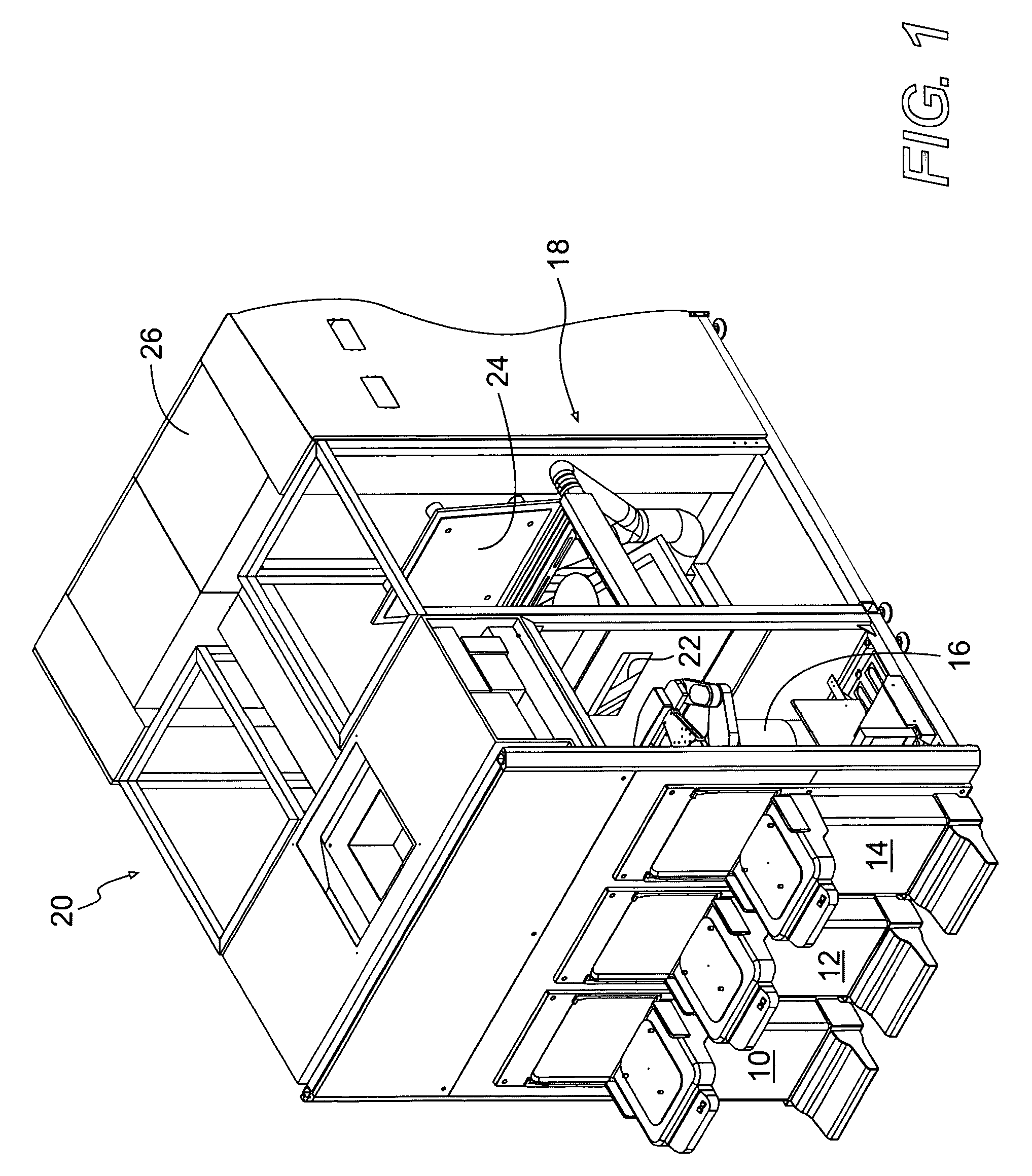
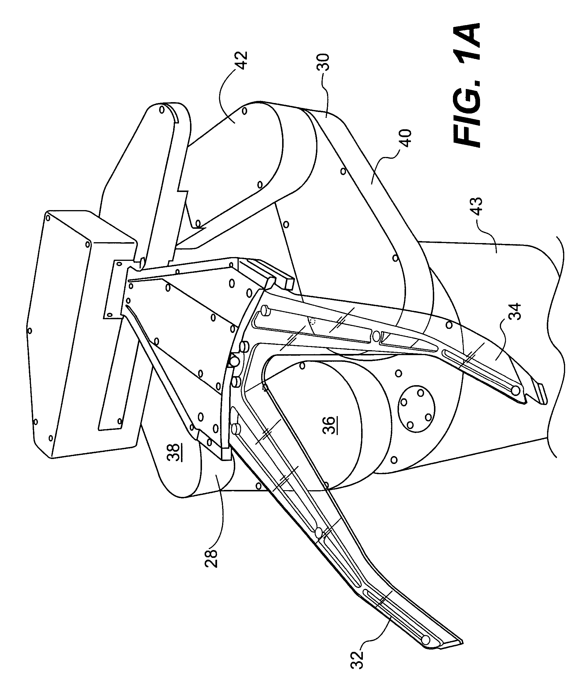
The present invention is directed to an improved design of an endeffector for handling semiconductor wafers. The new design has various advantages and benefits not previously realized in previous designs. The new design has a slim profile, with a maximum profile height of less than about 12 mm. It includes a base member with a first tine and a second tine in a forked arrangement. The base member has support members that can contact and support the wafer on its edges. The new design also includes a pushing device for positioning the wafer on the base member. The pushing device can have a retractable piston and a biasing member that can move the piston from its retracted position to its extended position. The new design also includes a suction device for capturing any particles released during movement of the piston. The new design can be used for handling cold or hot wafers, and it has a light detection system for detecting the presence of a wafer on the endeffector. The invention recognizes the need for improved design of the endeffector to improve its performance and reliability in the wafer processing system.

Problems solved by technology

For example, many wafer handling tools are relatively large and bulky in order to accommodate many of the instruments that are now attached to the tools in order to more precisely transport wafers.
The size of the endeffectors, however, limit the speed at which the endeffectors are transported and accelerated.
Further, relatively large endeffectors require that the processing chamber contain relatively large openings for receiving the endeffectors and the wafers carried thereon.

Method used


Image

  • Endeffectors for handling semiconductor wafers
  • Endeffectors for handling semiconductor wafers
  • Endeffectors for handling semiconductor wafers

Examples


Embodiment Construction

[0038]Reference now will be made to the embodiments of the invention, one or more examples of which are set forth below. Each example is provided by way of explanation of the invention, not as a limitation of the invention. In fact, it will be apparent to those skilled in the art that various modifications and variations may be made in the invention without departing from the scope or spirit of the invention. For instance, features illustrated or described as part of one embodiment may be used in another embodiment to yield a still further embodiment. Thus, it is intended that the present invention cover such modifications and variations as come within the scope of the appended claims and their equivalents. It is to be understood by one of ordinary skill in the art that the present discussion is a description of exemplary embodiments only, and is not intended as limiting the broader aspects of the present invention, which broader aspects are embodied in the exemplary constructions.

[...


PUM


Abstract

Various endeffector designs are disclosed for handling semiconductor wafers. For instance, an endeffector for handling wafers at a relatively low temperature is disclosed along with an endeffector for handling wafers at a relatively high temperature. Both endeffectors include uniquely designed support members that are configured to only contact a wafer at the wafer's edge. The endeffectors may also include a wafer detection system. The endeffector for handling wafers at relatively low temperatures may also include a pushing device that is used not only to position a wafer but to hold a wafer on the endeffector during acceleration or deceleration of the endeffector caused by a robot arm attached to the endeffector. As designed, the endeffectors may have a very slim profile making the endeffectors easily maneuverable.

Description

PRIORITY CLAIMS[0001]This application claims the benefit of U.S. Provisional Application No. 60 / 483,425, entitled “ENDEFFECTORS FOR HANDLING SEMICONDUCTOR WAFERS”, filed Jun. 27, 2003 and which is incorporated herein by reference for all purposes.BACKGROUND OF THE INVENTION[0002]In general, an integrated circuit refers to an electrical circuit contained on a single monolithic chip containing active and passive circuit elements. Integrated circuits are fabricated by diffusing and depositing successive layers of various materials in a preselected pattern on a substrate. The materials can include semiconductive materials such as silicon, conductive materials such as metals, and low dielectric materials such as silicon dioxide. The semiconductive materials contained in integrated circuit chips are used to form almost all of the ordinary electronic circuit elements, such as resistors, capacitors, diodes, and transistors.[0003]Typically, the substrate that is used to form integrated circu...

Claims


Application Information

Patent Timeline
Patent Type & Authority Patents(United States)
IPC IPC(8): B65G49/07B66C1/02H01L21/687
CPCH01L21/68707Y10S414/141H01L21/687
Inventor MANTZ, PAUL
Owner MATTSON TECHNOLOGY
Learn More