
Pixel structure and manufacturing method of liquid crystal display panel having the same

a technology pixel structure, which is applied in the field of pixel structure and manufacturing method of liquid crystal display panel having the pixel structure, can solve the problems of reduced contrast ratio of lcd panel, limited aperture ratio of display, and undesired tilting of parts of liquid crystal molecules, so as to reduce the disclination of the tilting direction

Active Publication Date: 2010-01-12
AU OPTRONICS CORP
View PDF2 Cites 2 Cited by
  • Summary
  • Abstract
  • Description
  • Claims
  • Application Information

AI Technical Summary

Benefits of technology

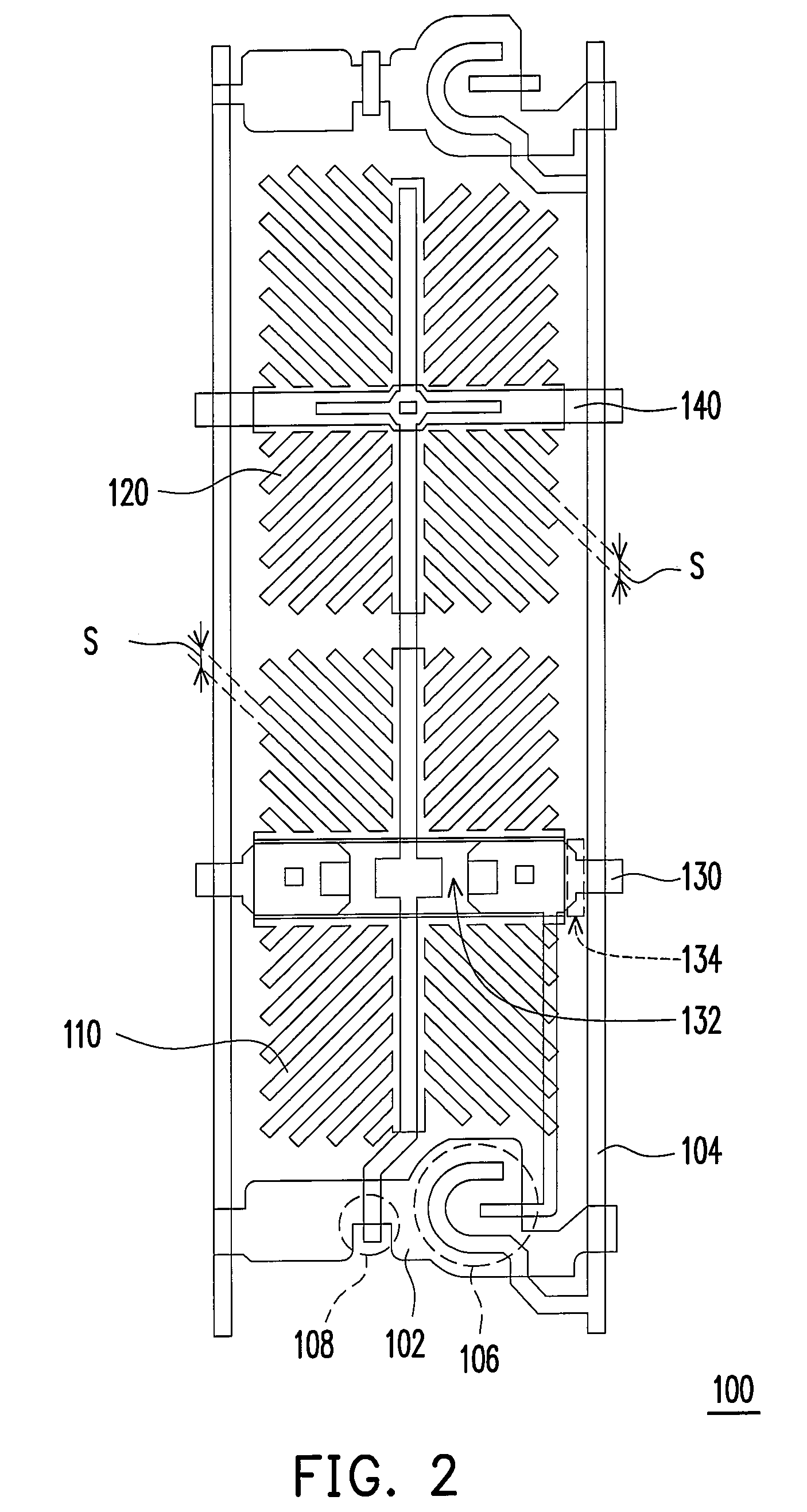
[0027]Through changing the patterns of the capacitance lower electrode in the pixel structure of the present invention, an area of the capacitance lower electrode uncovered by other conductive layers is reduced. Therefore, the pixel structure of the present invention is conducive to reducing disclination of the tilting direction of the liquid crystal molecules when applied to the PSA LCD panel. Moreover, the opening corresponding to a center of the pixel structure can be further formed in the conductive layer above the capacitance lower electrode according to the present invention, such that the liquid crystal molecules can be arranged in an appropriate direction in the PSA process.

Problems solved by technology

However, light leakage caused from disclination of a tilting direction of the liquid crystal molecules surrounding the alignment protrusions and the alignment slits frequently leads to a reduction of the contrast ratio of the LCD panel.
Nevertheless, an aperture ratio of the display is limited thereby.
Nevertheless, unfortunately, the process of achieving the PSA often gives rise to certain defects, thus bringing about undesired tilting of parts of the liquid crystal molecules.

Method used


Image

  • Pixel structure and manufacturing method of liquid crystal display panel having the same
  • Pixel structure and manufacturing method of liquid crystal display panel having the same
  • Pixel structure and manufacturing method of liquid crystal display panel having the same

Examples


first embodiment

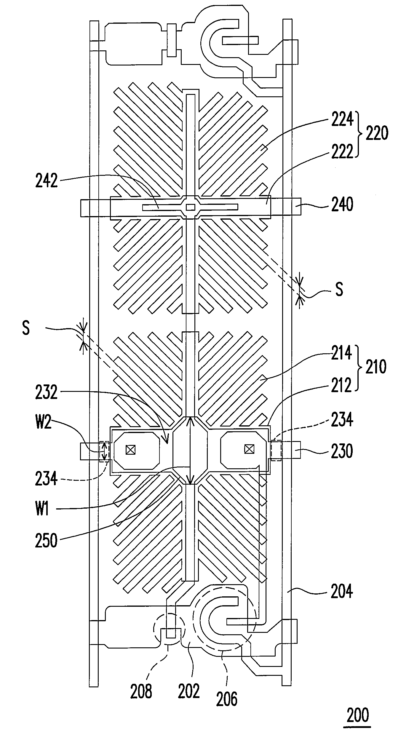
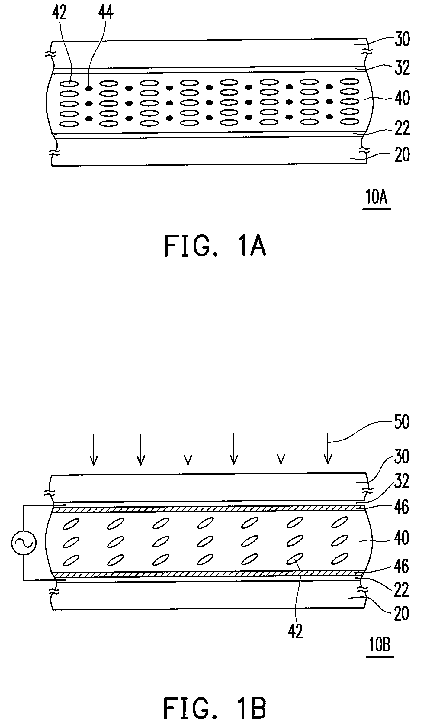
[0043]FIG. 3A is the pixel structure according to a first embodiment of the present invention. Referring to FIG. 3A, a pixel structure 200 electrically connects a an line 202 and a data line 204 and includes a first active device 206, a second active device 208, a first pixel electrode 210 electrically connecting the first active device 206, a second pixel electrode 220 electrically connecting the second active device 208 and a first capacitance lower electrode 230. Both the first active device 206 and the second active device 208 electrically connect the scan line 202 and the data line 204. As the pixel structure 200 is applied to the LCD panel 10B illustrated in FIG. 1B, the pixel array 22 can be formed by arranging a plurality of the pixel structures 200 on the array substrate 20.

[0044]The first pixel electrode 210 has a first interlacing pattern 212 and a plurality of first stripe patterns 214 connected to the first interlacing pattern 212. The second pixel electrode 220 has a s...

second embodiment

[0051]FIG. 4A is the pixel structure according to a second embodiment of the present invention. FIG. 4B is a cross-sectional view along a line A-A′ depicted in FIG. 4A. Referring to FIGS. 4A and 4B, the design of a pixel structure 300 is similar to the design of the pixel structure 200, and thus identical elements are not further described hereinafter. The difference therebetween lies in that a first capacitance upper electrode 350 of the pixel structure 300 has a first opening 352, while a first pixel electrode 310 has a second opening 316. In addition, the pattern design of the first capacitance lower electrode 330 is slightly different from that in the pixel structure 200.

[0052]It is observed from the cross-sectional view that the pixel structure 300 further includes an insulating layer 360 and a dielectric layer 370. The insulating layer 360 is disposed between the first capacitance lower electrode 330 and the first capacitance upper electrode 350. The dielectric layer 370 is di...


PUM

PropertyMeasurementUnit
voltageaaaaaaaaaa
AC voltageaaaaaaaaaa
electricallyaaaaaaaaaa

Abstract

A pixel structure including a first active device, a second active device, a first pixel electrode electrically connecting the first active device, a second pixel electrode electrically connecting the second active device and a first capacitance lower electrode is provided. Both the first active device and the second active device electrically connect a scan line and a data line. The first pixel electrode has a first interlacing pattern and first stripe patterns connected thereto. The second pixel electrode has a second interlacing pattern and second stripe patterns connected thereto. The first capacitance lower electrode located under the first interlacing pattern has a first region and second regions. The first pixel electrode substantially shields the first region but does not shield the second regions. An area ratio of the first region to the second regions is about 10:1˜300:1.

Description

CROSS-REFERENCE TO RELATED APPLICATION[0001]This application claims the priority benefit of Taiwan application serial no. 96139011, filed on Oct. 18, 2007. The entirety the above-mentioned patent application is hereby incorporated by reference herein and made a part of specification.BACKGROUND OF THE INVENTION[0002]1. Field of the Invention[0003]The present invention relates to a pixel structure and a manufacturing method of a liquid crystal display (LCD) panel having the pixel structure, and more particularly to a pixel structure in which liquid crystal molecules form a multi-domain alignment and a manufacturing method of the LCD panel having the pixel structure.[0004]2. Description of Related Art[0005]LCDs characterized by high contrast ratio, no gray scale inversion, little color shift, high luminance, full color, desirable color saturation, high responsive speed, and wide viewing angles are required in the market. At this current stage, some display panels, such as twisted nemat...

Claims


Application Information

Patent Timeline
Patent Type & Authority Patents(United States)
IPC IPC(8): G02F1/1343
CPCG02F1/133753G02F1/13439G02F1/133703G02F1/133788G02F2001/133749G02F2001/133757G02F2001/133765G02F2001/134345G02F2201/122G02F2202/025G02F1/133749G02F1/133765G02F1/133757G02F1/134345
Inventor CHEN, CHIEH-WEITSAO, CHENG-HANSU, JENN-JIA
Owner AU OPTRONICS CORP
Learn More