Electronic component comprising a cooling surface

Inactive Publication Date: 2009-12-15
ROHDE & SCHWARZ GMBH & CO KG
View PDF14 Cites 2 Cited by
  • Summary
  • Abstract
  • Description
  • Claims
  • Application Information

AI Technical Summary

Benefits of technology

[0007]The object of the invention is to provide an electronic component, which allows simple assembly on the surface of a printed-circuit board and a simplified arrangement of a cooling element, wherein the occurrence of a parasitic inductivity and / or capacity is avoided.
[0010]The further connecting elements can be guided in a straight line towards the surface of the printed-circuit board, because the further connecting elements are formed in the at least one recessed region of the first connecting element and because the contact surface of the first connecting element is formed in a raised region of the first connecting element. This not only shortens the entire signal path from the contact position on the printed-circuit board to the semiconductor substrate, which is connected with bonding wires to the individual connecting elements, but also achieves an improved geometry of the connecting elements and accordingly a reduction in parasitic inductivities and capacities by comparison with known components, which are provided for assembly on the surface of the printed-circuit board.
[0013]A further improvement of the shielding of the component is achieved in that the raised region surrounds the recessed region in the form of an enclosed ring. The flat cooling surface and the raised region therefore form a trough-like geometry, into which the remaining parts of the component are inserted. Placing the entire component on the printed-circuit board achieves an encapsulation of the component by the first connecting element, which is manufactured in metal, and accordingly a shielding by the electronic component itself, without the necessity for an additional cover.
[0014]Moreover, it is advantageous to form in the first connecting element several recessed regions, which can be provided, for example, by milling a cuboidal blank, wherein a semiconductor substrate is arranged in each of the recessed regions, and additionally, the further connecting elements necessary for each semiconductor substrate are formed in the corresponding recessed region. A symmetrical structure of this kind, known, for example, as a “push-pull” or “matched” structure, improves the performance of the electronic components in the high-frequency range and accordingly reduces the expenditure required for an adaptation network.
[0015]By contrast with the further connecting elements, the first connecting element is used in common for the entire semiconductor substrate of the electronic component, wherein, according to a particularly preferred embodiment, the first connecting element is a source connection of a field-effect transistor. As a result of the joint use of the first connecting element as a source connection for a field-effect transistor with several semiconductor substrates, the occurrence of potential differences between the respective source connections of the individual semiconductor substrates is advantageously avoided.
[0016]Furthermore, it is advantageous to design the entire surface of the electronic component facing away from the printed-circuit board as a flat cooling surface. In addition to the large contact surface between the cooling element and the electronic component, which favours heat transfer, in the context of the heat transfer between the flat surface and an adjoining housing structure, this also prevents the occurrence of a difference in the level of the flat cooling surface and the adjoining housing structure, which would prevent the cooling element from lying flush on the flat surface.

Problems solved by technology

A folding of the connecting elements is disadvantageous, especially for applications in the high-frequency range.
The curved geometry of the connecting elements generates a high parasitic inductivity and possibly also parasitic capacity, which reduce the useful frequency range.

Method used


Image

  • Electronic component comprising a cooling surface
  • Electronic component comprising a cooling surface
  • Electronic component comprising a cooling surface

Examples


Embodiment Construction

)

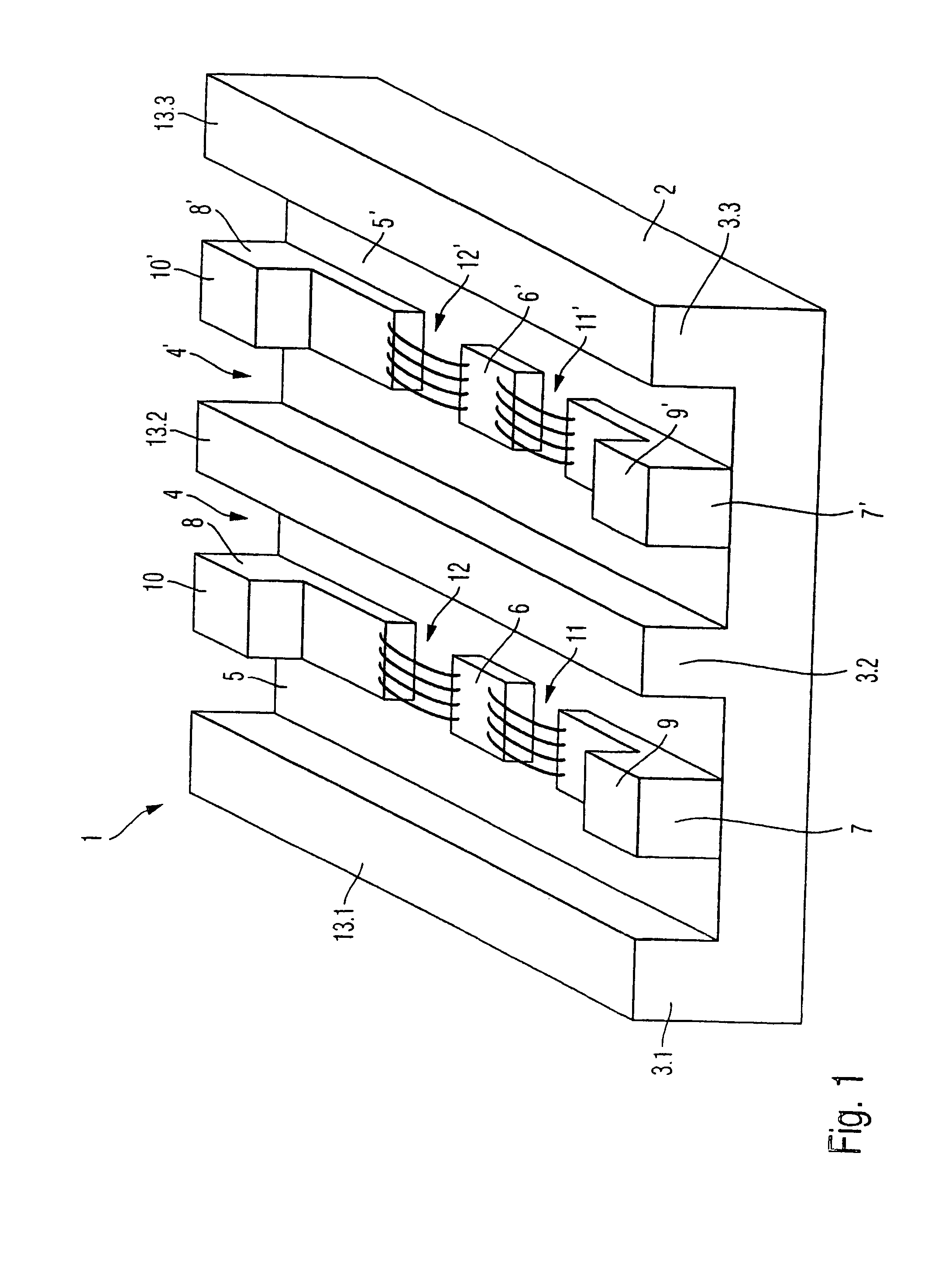
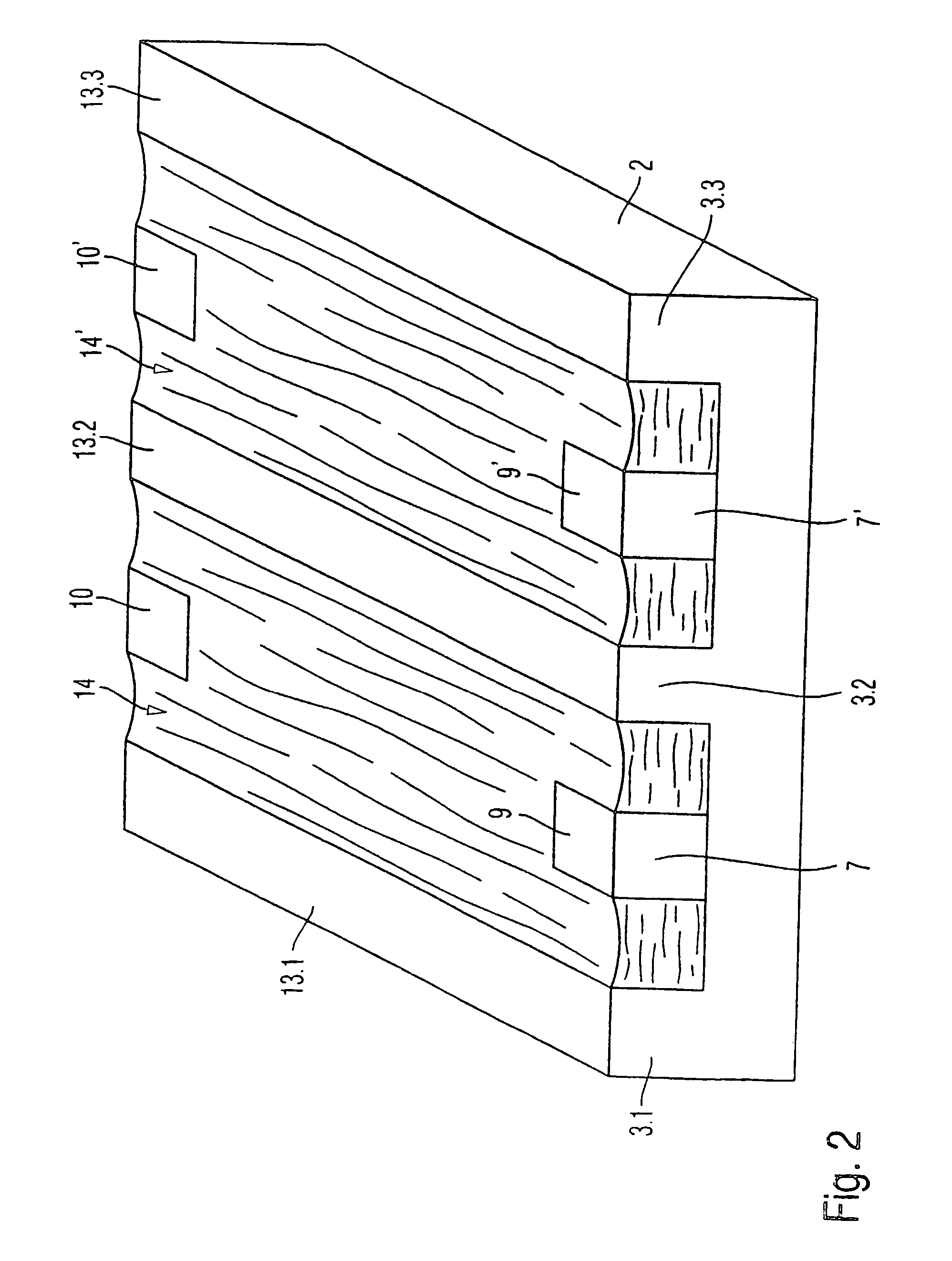
[0025]FIG. 1 shows a first exemplary embodiment of an electronic component 1 according to the invention. A substantial part of the housing of the electronic component 1 is formed by a first connecting element 2. In the first exemplary embodiment, the first connecting element 2 is formed with a rectangular base surface. Parallel to an outer edge of the rectangular base surface, a first raised region 3.1, a second raised region 3.2 and a third raised region 3.3 are formed on the side of the electronic component 1, which will be arranged on the printed-circuit board after assembly. The three raised regions 3.1, 3.2 and 3.3 are distributed uniformly over the base surface of the first connecting element 2.

[0026]A recessed region 4 and respectively 4′ is formed between the adjacent raised regions, that is to say, between the first raised region 3.1 and the second raised region 3.2, and between the second raised region 3.2 and the third raised region 3.3 respectively. These recessed regio...


PUM


Abstract

An electronic component comprising at least two connection elements (2,7,8), each provided with at least one contact surface (13.1, 13.2, 13.3, 9, 10) which is used to fix the electronic component (1) to a surface of a printed circuit board. An at least partially plane cooling surface is formed on the first connection element (2), for placing on a cooling body that is oriented in the direction of the side of the electronic component (1) opposing the printed circuit board. The first connection element (2) has at least one raised area (3.1, 3.2, 3.3) on the side thereof facing the printed circuit board, on which the contact surface (13.1, 13.2, 13.1) of the first connection element (2) is formed. Said first connection element (2) also has at least one recessed area (4, 4′) in which the at least one other connection element (7, 7′; 8, 8′) is arranged.

Description

CROSS REFERENCE TO RELATED APPLICATIONS[0001]This application claims priority to German Patent Application Serial No.: DE102004004074.5 filed Jan. 27, 2004 and German Patent Application Serial No.: DE10341081.3 filed Sep. 5, 2003.BACKGROUND[0002]1. Field of the Invention[0003]The invention relates to an electronic component for assembly on the surface of a printed-circuit board, especially a power transistor for high-frequency applications.[0004]2. Description of the Related Art[0005]Electronic components, especially power transistors, which are mounted on the surface of a printed-circuit board, are already known. If these components must be cooled during operation, a mounting, by means of which a cooling element can be attached to the component, must be provided on the component in addition to the contact surfaces of the component. A high-frequency power transistor with a synthetic-material housing is known, for example, from the technical datasheet “MRF 1535T1 / D”, Motorola Inc. Co...

Claims


Application Information

Patent Timeline
IPC IPC(8): H01L23/66H01L23/049H01L23/24H01L23/367H01L23/495H01L23/498H01L23/552
CPCH01L23/24H01L23/3675H01L23/49805H01L23/552H01L24/49H01L2924/1306H01L2924/014H01L2924/01072H01L2224/48091H01L2224/49175H01L2924/01005H01L2924/01082H01L2924/1532H01L2924/30107H01L2924/3025H01L24/48H01L2924/01033H01L2924/00014H01L2924/00H01L2924/181H01L2224/45099H01L2924/00012
Inventor FLUHRER, CHRISTOPHSCHNIEDER, HERBERT
Owner ROHDE & SCHWARZ GMBH & CO KG
Why Eureka
Try Eureka