Image sensor, driving method and camera
a driving method and image sensor technology, applied in the field of image sensors, can solve the problem that the output signal of electronic shutters cannot be arbitrary, and achieve the effect of less voltage margin
- Summary
- Abstract
- Description
- Claims
- Application Information
AI Technical Summary
Benefits of technology
Problems solved by technology
Method used
Image
Examples
first embodiment
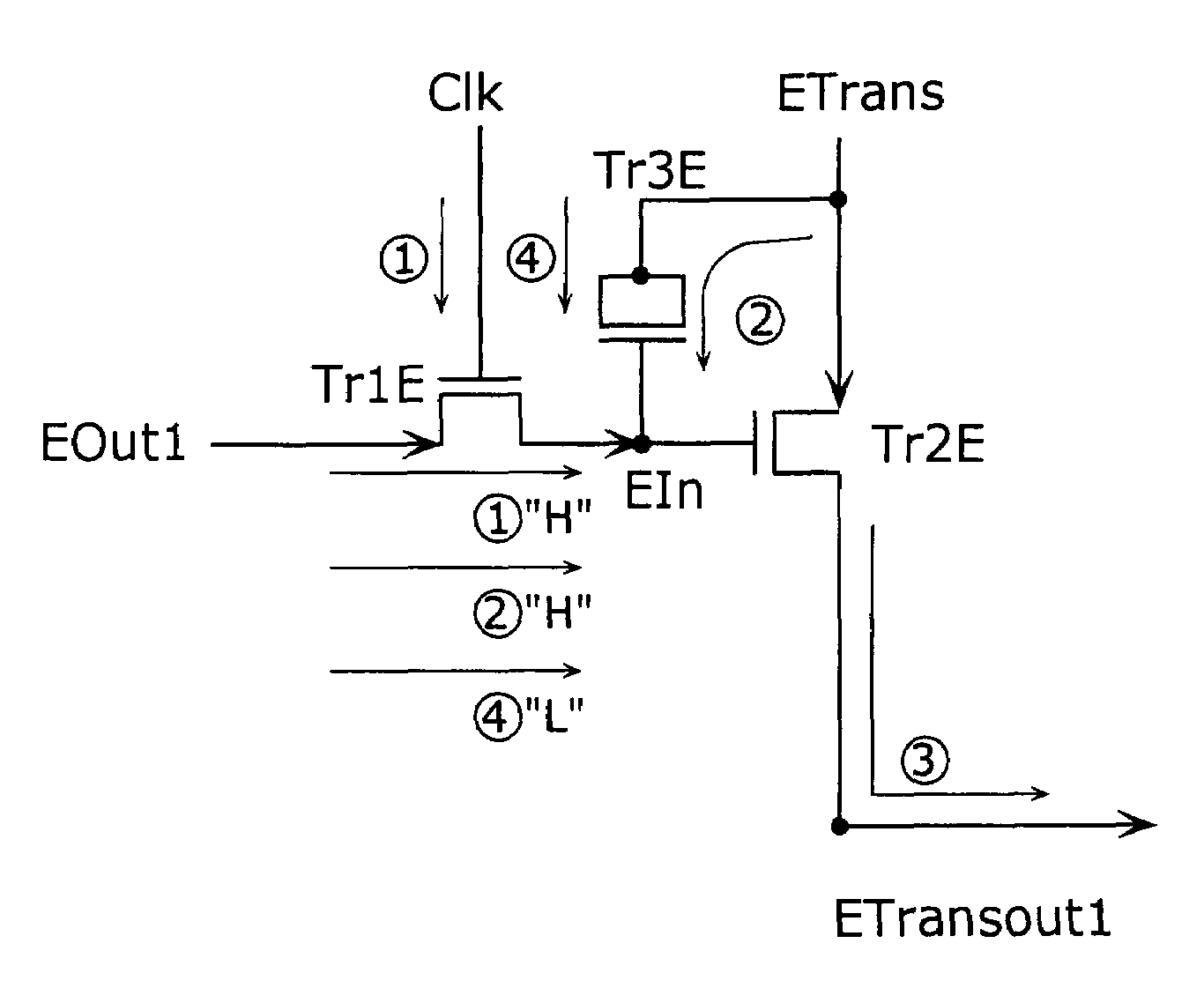
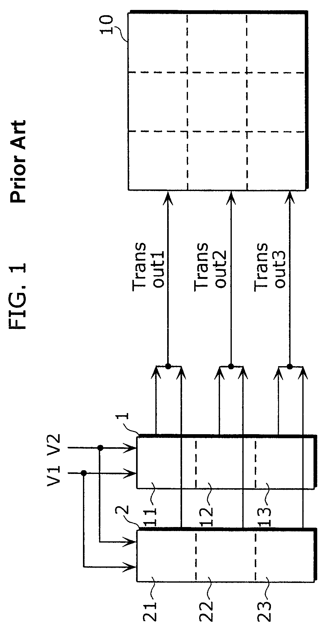
[0047]FIG. 4 is a sketchy diagram showing the main part of the image sensor according to the first embodiment of the present invention. The image sensor is composed of: a scanning circuit 1 for performing normal scanning; a scanning circuit 2 for performing scanning for electronic shutter use; a selection circuit 3 for selecting an output signal outputted from the scanning circuits 1, 2, and outputting it at an arbitrary timing; and the sensor unit 10 being made up of a plurality of pixels. The scanning circuits 1, 2 and the sensor unit 10 are as same as those described in FIG. 1 and the structure of the unit register constituting the scanning circuits 1, 2 is as same as the one described in FIG. 2A, therefore, the descriptions are omitted here. The TRANS and ETRANS signals in FIG. 1 are control signals for specifying the output signal outputted from the scanning circuits 1, 2 as well as the timing to output the output signal.
[0048]The selection circuit 3 holds the output signal Out...
second embodiment
[0067]The present embodiment will describe an image sensor which overcomes the problem caused by the threshold of the switching transistor Tr1E that is too low, as mentioned in the first embodiment. The structure of the image sensor is the same as the one shown in FIG. 4 and the structure of the unit selection circuit is as same as the one shown in FIG. 5A, so those descriptions are omitted here. The image sensor according to the present embodiment differs from the one described in the first embodiment in the respect that the pulse duration of the clock signals V1 and V2 are widened to make up a great part of one horizontal period.
[0068]In FIGS. 8A and 8B, the output signal EOut at a high level is held in the gate capacitor of the boosting transistor Tr2E with the timing shown in {circle around (1)}. The voltage is applied to the pulse ETrans so that the output signal EOut is outputted with the timing shown in {circle around (2)}. Here, since the output signal EOut is held at a high...
third embodiment
[0075]FIG. 10 is a diagram showing the schematic structure of the main part of the image sensor according to the third embodiment. The structure shown in the diagram is different from the one shown in FIG. 4 in the respect that it includes a selection circuit 3a instead of the selection circuit 3. The selection circuit 3a does not require the clock signal Clk, which is different from the selection circuit 3a. The following focuses on the difference and the description for components which are the same is omitted.
[0076]FIG. 11 is a circuit diagram showing the structure of the selection circuit 3a. The power supply VDD, instead of the clock signal Clk, is connected to the gate of the switching transistor Tr1E.
[0077]FIGS. 12A˜12C are illustrations showing the operation of the selection circuit 3a. As in the second embodiment, the pulse durations of the clock signals V1, V2 are widened to make up a great part of one horizontal scanning period. It thus solves the problem that the boostin...
PUM
 Abstract
Description
Claims
Application Information
 - R&D
- Intellectual Property
- Life Sciences
- Materials
- Tech Scout
- Unparalleled Data Quality
- Higher Quality Content
- 60% Fewer Hallucinations
Browse by: Latest US Patents, China's latest patents, Technical Efficacy Thesaurus, Application Domain, Technology Topic, Popular Technical Reports.
© 2025 PatSnap. All rights reserved.Legal|Privacy policy|Modern Slavery Act Transparency Statement|Sitemap|About US| Contact US: help@patsnap.com


