Multi-mode optical coherence device and fabrication method thereof

a multi-mode optical coherence and interference technology, applied in the direction of optical waveguide light guide, instruments, optics, etc., can solve the problems of reducing reflection, affecting the character of light source connected to this single-mode waveguide, and unable to completely eliminate reflection influence, so as to achieve the effect of eliminating the effect of reflected light and simple structur

Active Publication Date: 2009-09-22
NEOPHOTONICS CORP
View PDF13 Cites 0 Cited by
  • Summary
  • Abstract
  • Description
  • Claims
  • Application Information

AI Technical Summary

Benefits of technology

[0011]The present invention has a purpose to provide an MMI device which is capable of completely eliminating the return of the reflected light with a simple structure, and a manufacturing method for the same.
[0013]With the present invention, at both ends of the multimode waveguide, a wall face perpendicular to the optical axis direction that is not provided with the single-mode waveguide is formed so as to have an inclination in the thickness direction. Thereby, the light incident on the wall face perpendicular to the optical axis direction is reflected toward the substrate surface side, irradiating onto the substrate surface at a small incident angle. Therefore, the light irradiating onto the substrate surface is not reflected at the substrate surface, but is irradiated into the substrate, and is not returned to the waveguide. Therefore, an effect that, with a simple structure, the return of the reflected light can be completely eliminated, is provided.

Problems solved by technology

However, it is known, with the MMI device as shown in FIG. 2A, that the light which is introduced into the single-mode waveguide A and is passed through the multimode waveguide M is incident on the perpendicular end face T2 at the light emission end, and a part of the light is reflected to be returned to the single-mode waveguide A, resulting in the characteristics of the light source connected to this single-mode waveguide A being adversely influenced.
Further, a part of the reflected light is returned to the single-mode waveguide A. Therefore, there has been presented a problem that, while compared to the MMI device as shown in FIG. 2A the influence of the reflection is reduced, the influence of the reflection cannot be completely eliminated.

Method used


Image

  • Multi-mode optical coherence device and fabrication method thereof
  • Multi-mode optical coherence device and fabrication method thereof
  • Multi-mode optical coherence device and fabrication method thereof

Examples


exemplary embodiment 1

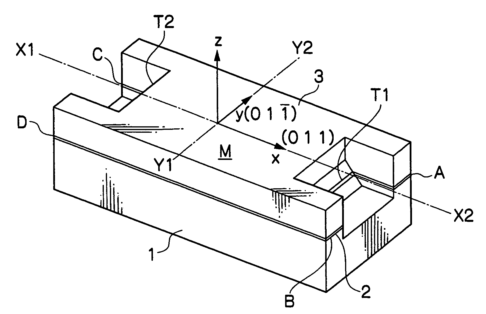
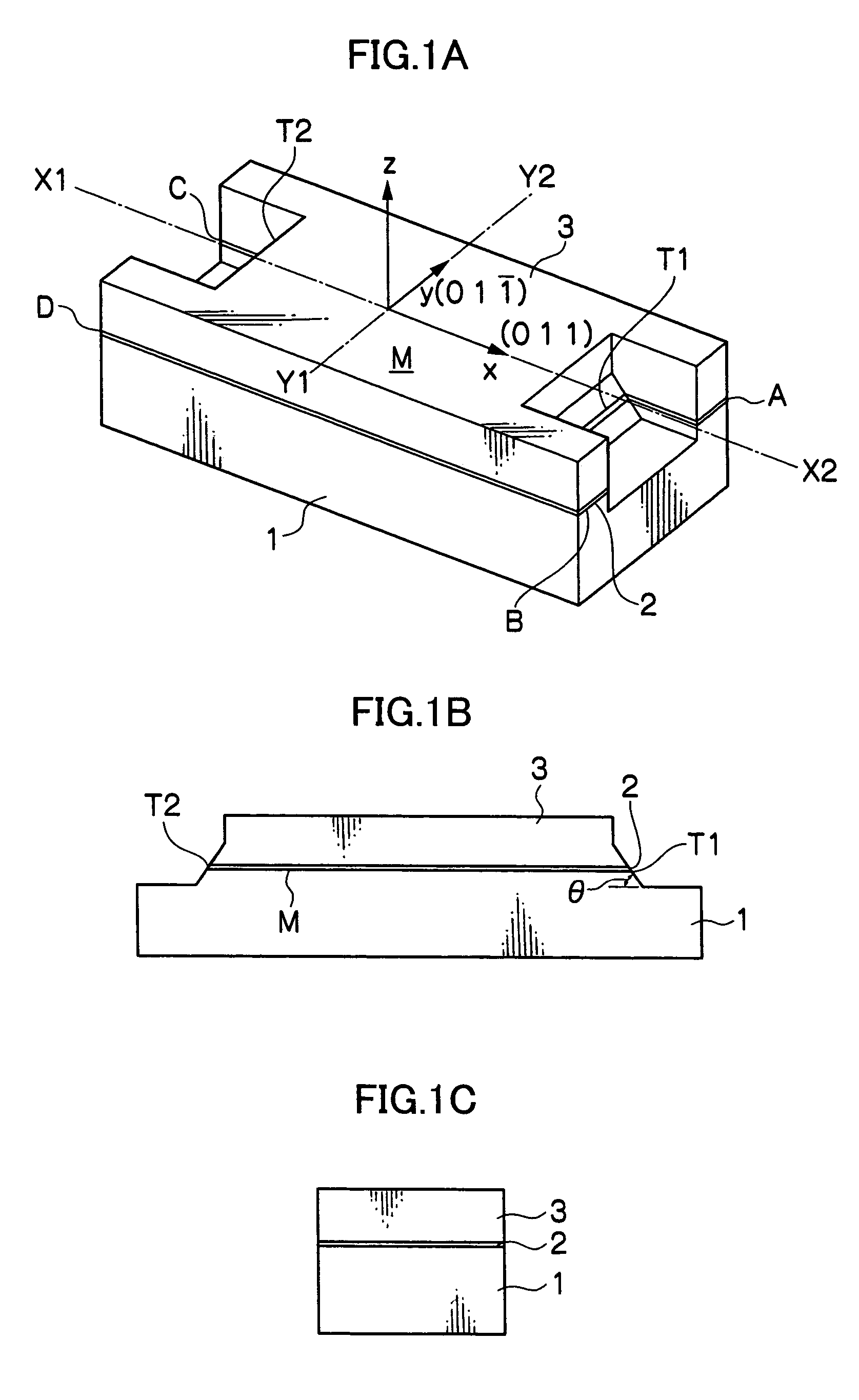
[0027]FIG. 1A to FIG. 1C are structural diagrams illustrating an MMI device of an exemplary embodiment of the present invention, FIG. 1A being a perspective view, FIG. 1B a sectional view of a portion along the line X1-X2 in FIG. 1A, and FIG. 1C a sectional view of a portion along the line Y1-Y2 in FIG. 1A.

[0028]This MMI device is formed by sequentially layering a light guiding layer 2 constituting a waveguide with an InGaAsP crystal having a thickness of about 0.5 μm on a substrate 1 made of an InP crystal which is a lower cladding layer, and an upper cladding layer 3 made of an InP crystal having a thickness of 2 to 4 μm, and working this to a geometry of a substantially rectangular parallelepiped having a length of 100 to 500 μm, and a width of about 15 to 100 μm.

[0029]As shown in FIG. 1A, the XY surface of the rectangular parallelepiped is set such that the X-axis direction corresponds to a plane defined by the crystal direction (0 1 1), and the Y-axis direction to a plane defin...


PUM


Abstract

In an MMI device with which a plurality of narrow width single-mode waveguides are provided at both ends of a multimode waveguide M, and light introduced into one single-mode waveguide on the input side is interfered in the multimode waveguide to be emitted from two single-mode waveguides on the output side, a wall face perpendicular to the optical axis direction that is not provided with a single-mode waveguide is formed with an inclination being given in the thickness direction, at both ends of the multimode waveguide. Thereby, the light which is incident on the wall face is reflected toward the substrate side. In this case, because the angle of incidence into the substrate is small, almost all of the light is radiated into the inside of the substrate without being returned to the single-mode waveguide on the incident side. Therefore, an MMI device which is capable of completely eliminating the return of the reflected light with a simple structure, and a manufacturing method for the same are provided.

Description

CROSS-REFERENCE TO RELATED APPLICATION[0001]This application claims priority under 35 USC 119 from Japanese Patent Application No. 2005-351802, the disclosure of which is incorporated by reference herein.BACKGROUND OF THE INVENTION[0002]1. Field of the Invention[0003]The present invention relates to an optical multimode interference device (hereinafter called an “MMI” device), and a manufacturing method for the same, to be used in optical communication, optical switching, optical wiring, and the like.[0004]2. Description of the Related Art[0005]FIG. 2A and FIG. 2B shows a plan view illustrating the structure of a conventional MMI device. Literature that discloses the conventional art includes Japanese Patent Laid-Open Publication No. 2001-215452, and U.S. Pat. No. 5,563,968.[0006]With the conventional MMI device as shown in FIG. 2A, for example, narrow width single-mode waveguides A, B are provided at one end in a longitudinal direction of a rectangular parallelepiped forming a wave...

Claims


Application Information

Patent Timeline
Patent Type & Authority Patents(United States)
IPC IPC(8): G02B6/26G02B6/10G02B6/42
CPCG02B6/2813
Inventor WADA, HIROSHI
Owner NEOPHOTONICS CORP
Why Eureka
Try Eureka