
Integrated circuit monitoring an internal signal converted from an analog input signal

a technology of integrated circuits and input signals, applied in the field of integrated circuits, can solve the problems of increasing the cost of lsi unintentionally, difficult to evaluate functional blocks or perform debugging, and difficulty in evaluating functional blocks or performing debugging, so as to achieve the effect of reducing the manufacturing cost and the overall dimensions of the integrated circui

Active Publication Date: 2009-09-01
PANASONIC CORP
View PDF11 Cites 0 Cited by
  • Summary
  • Abstract
  • Description
  • Claims
  • Application Information

AI Technical Summary

Benefits of technology

[0029]According to various preferred embodiments of the present invention described above, an internal signal of an integrated circuit can be monitored, and debugging and evaluation both can be done on the integrated circuit, even without providing any dedicated monitor terminal for the integrated circuit. Also, since no signals are output through any monitor terminal, the internal signal never makes noise that affects the operation of the integrated circuit. Furthermore, by omitting the monitor terminals, the manufacturing cost and overall dimensions of the integrated circuit can be both reduced, too.

Problems solved by technology

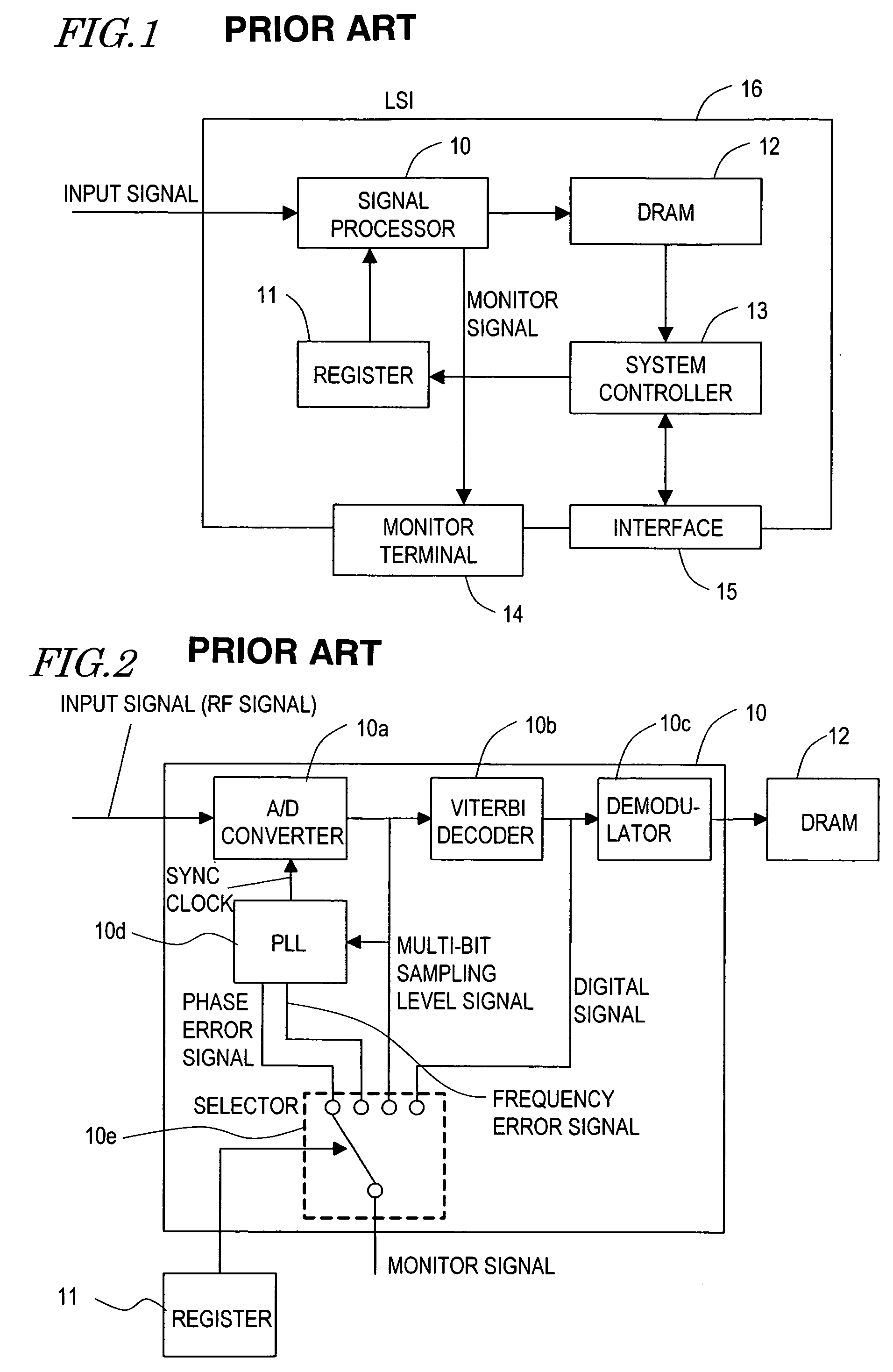
However, when multiple LSIs are packaged in a single chip, those functional blocks are interconnected together inside of the single-chip LSI and various signals to be exchanged between those blocks cannot be easily monitored externally, thus making it difficult to evaluate the functional blocks or perform debugging.
However, if those monitor terminals are provided, the number of overall terminals increases, thus raising the cost of the LSI unintentionally.
Nevertheless, even if the monitor signal is output in series, at least one terminal dedicated to monitoring is still required, thus increasing the cost of the LSI to a certain degree.
In that case, the current flowing through the monitor terminal will change so frequently as to increase the noise of the LSI noticeably.
Such noise may cause some malfunctions in an LSI that should operate at a sufficiently high rate.
Furthermore, if the monitor signal is output to monitor the internal states of the LSI, then the operation of the LSI might be affected by the noise caused by the monitor signal.

Method used


Image

  • Integrated circuit monitoring an internal signal converted from an analog input signal
  • Integrated circuit monitoring an internal signal converted from an analog input signal
  • Integrated circuit monitoring an internal signal converted from an analog input signal

Examples


embodiment 1

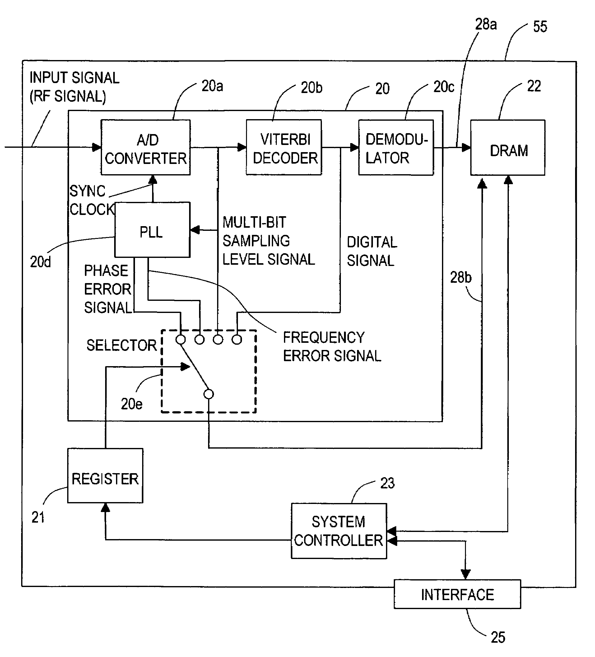
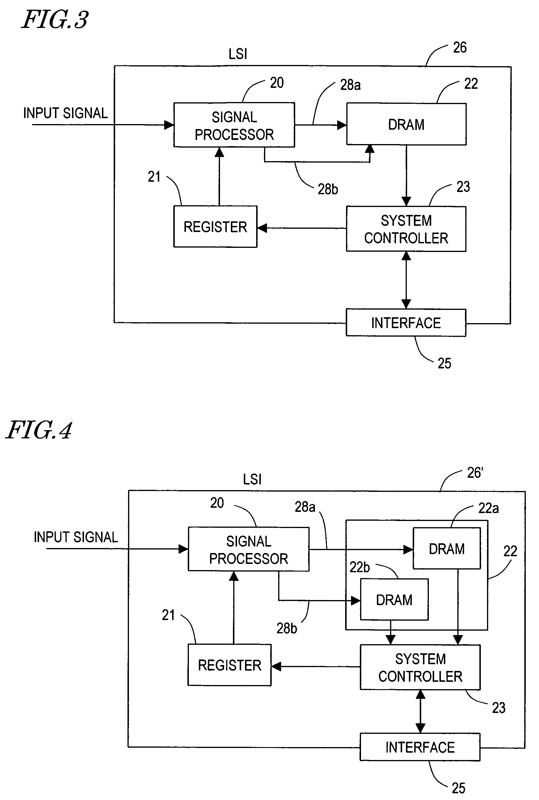
[0040]FIG. 3 is a block diagram showing an integrated circuit (which will be referred to herein as an “LSI”) according to a first specific preferred embodiment of the present invention. As shown in FIG. 3, the LSI 26 preferably includes a signal processor 20, a register 21, a DRAM 22 as at least one memory, a system controller 23, and an interface 25 with multiple terminals. All of these components of the LSI 26 are packaged together with a resin, for example, thereby making a single chip. Also, those terminals of the interface 25 preferably extend out of the package.

[0041]The signal processor 20 preferably receives an input signal and generates a processed signal, representing processing information, by subjecting the input signal to predetermined processing. The signal processor 20 also generates an internal signal including internal information obtained while performing the processing. The contents of the processing to be carried out by the signal processor 20 are preferably dete...

embodiment 2

[0061]FIG. 7 is a block diagram showing an LSI according to a second specific preferred embodiment of the present invention. As shown in FIG. 7, the LSI 36 preferably includes a signal processor 30, a register 31, a DRAM 32 as at least one memory, a system controller 33 and an interface 35 with multiple terminals. Each of the signal processor 30, DRAM 32 and interface 35 preferably has the same configuration as the counterpart of the first preferred embodiment described above.

[0062]In this second preferred embodiment, the internal signal generated by the signal processor 30 is preferably temporarily stored in the register 31 and then transferred to the DRAM 32 by way of the system controller 33. More specifically, the register 31 preferably includes a first register section 31a, on which a value defining the contents of processing to be performed by the signal processor 30 is specified, and a second register section31b, in which the internal signal is stored temporarily. The interna...


PUM

PropertyMeasurementUnit
timeaaaaaaaaaa
speedaaaaaaaaaa
frequencyaaaaaaaaaa

Abstract

An integrated circuit includes: a signal processor, which receives an input signal and generates a processed signal, representing processing information obtained by subjecting the input signal to predetermined processing, and at least one type of internal signal including internal information obtained during the processing; at least one memory storing the processing information; an interface exchanges signals with an external device; and a controller controlling the signal processor, memory and interface. On receiving a first instruction from the external device through the interface, the controller controls the signal processor and memory such that the processing information is once stored in the memory and then output to the external device via the interface. In response to a second instruction, the controller controls the signal processor and memory such that the internal information is once stored in the memory and then output to the external device via the interface.

Description

BACKGROUND OF THE INVENTION[0001]1. Field of the Invention[0002]The present invention relates to an integrated circuit that allows the user to monitor its internal signals.[0003]2. Description of the Related Art[0004]As information and communication technologies have been tremendously developing these days, it has become increasingly necessary to process a huge amount of information at a very high speed. To achieve this purpose, semiconductor integrated circuits for use in a data storage system or a communications system (e.g., multiple LSIs having the capability of processing analog and digital signals) are often combined together into a single semiconductor chip (which implementation will be referred to herein as a “single-chip LSI”).[0005]If multiple LSIs can be packaged in a single-chip LSI, then the number of electronic components needed to achieve their intended functions can be reduced significantly and the final circuit configuration can be simplified drastically, too. Also,...

Claims


Application Information

Patent Timeline
Patent Type & Authority Patents(United States)
IPC IPC(8): G06F13/12G06F13/00G06F3/00G11B7/085G11B20/10G01R31/28G11B27/36
CPCG01R31/3177G11B20/10
Inventor KIMURA, NAOHIROMIYASHITA, HARUMITSUNAKAJIMA, TAKESHIISHIBASHI, HIROMICHIYAMAMOTO, YOSHIKAZUNAKATA, KOHEI
Owner PANASONIC CORP
Learn More