
Data reading circuit

a data reading and circuit technology, applied in the field of data reading circuits, can solve the problems of data reading clock signal delay, complicated connection lines of electronic devices, and even more serious problems, and achieve the effect of reducing the error of data reading due to signal delay

Active Publication Date: 2009-09-01
REALTEK SEMICON CORP
View PDF10 Cites 0 Cited by
  • Summary
  • Abstract
  • Description
  • Claims
  • Application Information

AI Technical Summary

Benefits of technology

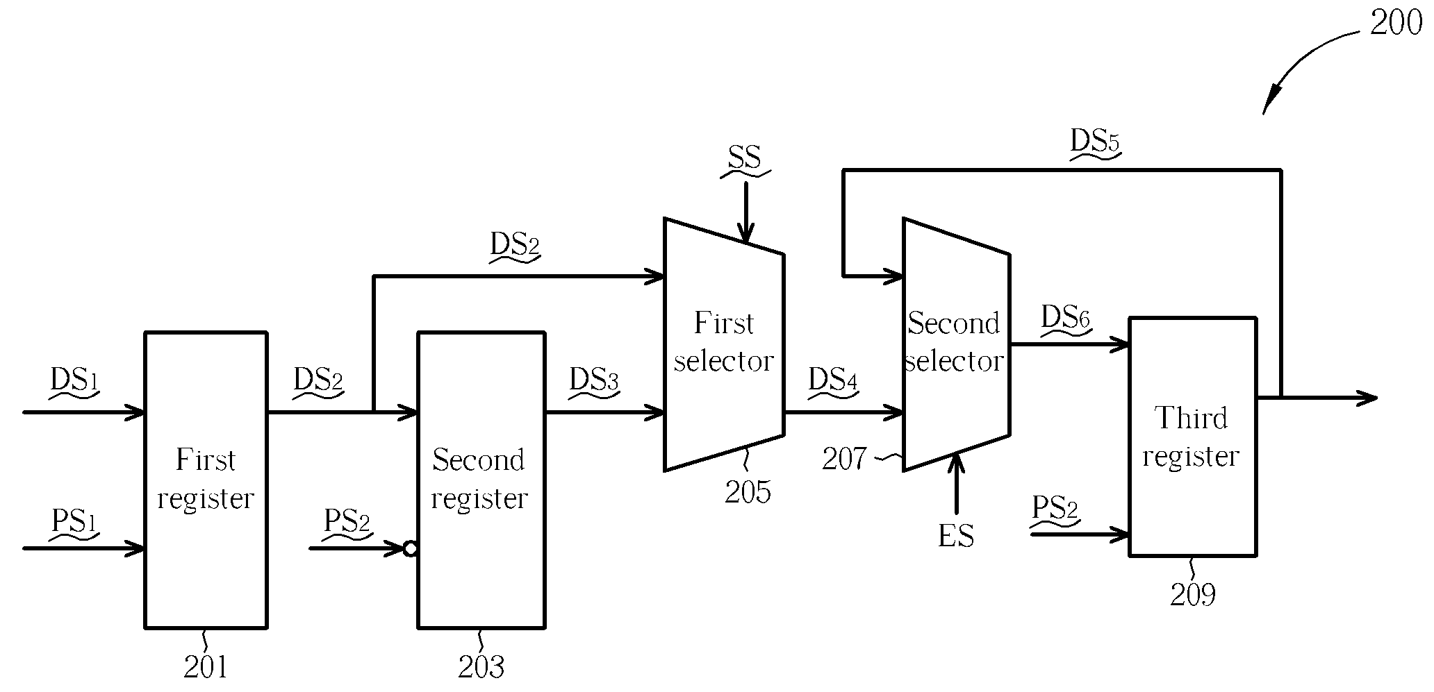
The present invention provides a data reading circuit and method that can adjust read data by multiple signals with specific relations to decrease data reading error due to signal delay. The circuit includes a first register, a second register, a first selector, a second selector, and a third register. The method involves receiving a first data signal, sampling it according to the first edges of a first predetermined signal, and selecting one of the second or third data signals as a fourth data signal based on the phases of the first and second predetermined signals. The circuit and method can adjust data read regardless of the frequency or delay of the data reading signal.

Problems solved by technology

The elements and connection lines of an electronic apparatus become complicated as related techniques improve, however, potentially resulting in delay of the data reading clock signal.
Such an error may be caused by the delay when reading data through a pad.
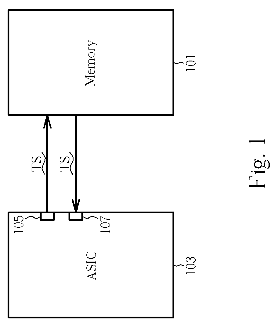
If the memory is used for ASICs (Application Specific Integrated Circuit), such a problem becomes even more serious.
Because each ASIC has its different characteristics, the system may be unstable and a design error will occur if the problem of a delayed data read clock signal is not solved.
Moreover, an extra step for simulating delay is also necessary, and the loading of the system thereby increases.

Method used


Image

  • Data reading circuit
  • Data reading circuit
  • Data reading circuit

Examples


Embodiment Construction

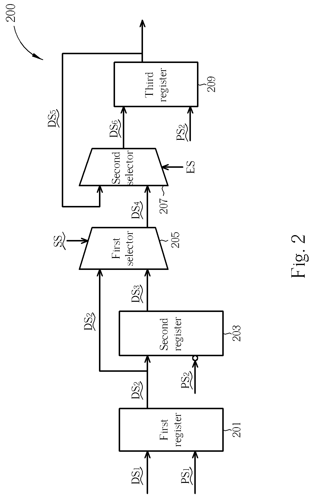
[0022]FIG. 2 is a diagram of the data reading circuit 200 illustrated according to a preferred embodiment of the present invention. As shown in FIG. 2, the data reading circuit 200 includes a first register 201, a second register 203, a first selector 205, a second selector 207, and a third register 209. The first register 201 is used for receiving a first data signal DS1 and for sampling the first data signal DS1 according to the first edges of a first predetermined signal PS1 to generate a second data signal DS2. The second register 203, which is coupled to the first register 201, is used for sampling the second data signal DS2 according to the second edges of a second predetermined signal PS2 to generate a third data signal DS3. The first selector 205, which is coupled to the second register 203, is used for selecting the second data signal DS2 or the third data signal DS3 as a fourth data signal DS4, which is in accordance with a selecting signal SS, wherein the selecting signal...


PUM


Abstract

Disclosed is a data reading circuit, including: a first register, for receiving a first data signal and generating a second data signal by sampling the first data signal via the first edge of a first predetermined signal; a second register, for sampling a second data signal by the second edge of a second predetermined signal to generate a third data signal; a first selector, for selecting one of the second and third data signals as a fourth data signal according to the phase difference between the first and second predetermined signals; a second selector, for selecting one of the fourth and a fifth data signals as a sixth data signal according to a selecting signal; and a third register, for sampling the sixth data signal to form the fifth data signal according to the first edge of the second predetermined signal.

Description

BACKGROUND OF THE INVENTION[0001]1. Field of the Invention[0002]The present invention relates to a data reading circuit, and particularly relates to a data reading circuit which adjusts according to a delay state of the data reading clock signal of the memory.[0003]2. Description of the Prior Art[0004]In modern electronics, a memory is used for storing various kinds of data, where a data reading clock signal is used for reading the data in the memory. The elements and connection lines of an electronic apparatus become complicated as related techniques improve, however, potentially resulting in delay of the data reading clock signal. Such an error may be caused by the delay when reading data through a pad. If the memory is used for ASICs (Application Specific Integrated Circuit), such a problem becomes even more serious. Because each ASIC has its different characteristics, the system may be unstable and a design error will occur if the problem of a delayed data read clock signal is n...

Claims


Application Information

Patent Timeline
Patent Type & Authority Patents(United States)
IPC IPC(8): G11C7/00
CPCG06F13/1689
Inventor KUO, TUNG-CHEN
Owner REALTEK SEMICON CORP
Learn More