Integrated photoreceptor circuit and optoelectronic component including the same with electric contact pads arranged solely on side of the processing area which is juxtaposed with the photosensitive area

a photoreceptor circuit and optoelectronic technology, applied in the direction of photometry, amplifiers controlled by light, photometry, etc., can solve the problems of wasting space and not using the photoreceptor circui

Active Publication Date: 2009-08-25
EM MICROELECTRONIC-MARIN
View PDF8 Cites 0 Cited by
  • Summary
  • Abstract
  • Description
  • Claims
  • Application Information

AI Technical Summary

Benefits of technology

[0008]It is thus an object of the invention to provide an integrated photoreceptor circuit that overcomes all the drawbacks of the aforecited prior art, wherein the particular arrangement of the various elements allows the size of the photoreceptor circuit to be reduced and certain parts of the circuit to be made symmetrical or balanced.
[0013]Advantageously, metal bumps are made on the contact pads to project from a passivation layer of the integrated photoreceptor circuit. These metal bumps, which are symmetrically distributed in the processing unit area, are for direct connection to corresponding contact pads of a printed circuit substrate or support by a flip chip technique. In order to do this, the connection pads of the substrate have the same arrangement and position as the metal bumps. Owing to this arrangement of metal bumps in the processing unit area, the assembly force of the circuit onto the substrate is applied only on the back of the processing unit area, leaving the photosensitive area free and without any assembly mechanical stress. The contact pressure due to the assembly force of the circuit with metal bumps onto the substrate is thus distributed in a suitable manner or in a balanced way. A reliable assembly is thus achieved while leaving the photosensitive part of the integrated circuit floating.
[0017]One advantage of the optoelectronic component according to the invention lies in the fact that it includes connection pads on a printed circuit substrate for connection to contact pads of the integrated photoreceptor circuit arranged opposite the processing unit area of the circuit. Thus, during an operation of electrically connecting the contact pads of the circuit to the connection pads of the substrate, any mechanical contact with the photosensitive area is avoided, leaving the latter free in order to protect it.
[0019]Advantageously, if the integrated photoreceptor circuit includes metal bumps, the first portion of the flexible substrate includes connection pads having the same arrangement and position as the metal bumps. In this manner, the integrated photoreceptor circuit can be mounted on the first portion by a flip chip technique, using a force applied only to the back of the processing unit area. Owing to the arrangement of the metal bumps of the circuit and the first portion of the substrate, this ensures a reliable assembly of the circuit on the substrate.

Problems solved by technology

With this distribution of the two areas of the photoreceptor circuit, the electric contact pads of the photoreceptor circuit are generally distributed all around the photosensitive area for example in a uniform manner, which leads to a waste of space.
Consequently, the photoreceptor circuit is not made in an optimum manner to satisfy current requirements to reduce the size of any optoelectronic component made, which is a drawback.

Method used


Image

  • Integrated photoreceptor circuit and optoelectronic component including the same with electric contact pads arranged solely on side of the processing area which is juxtaposed with the photosensitive area
  • Integrated photoreceptor circuit and optoelectronic component including the same with electric contact pads arranged solely on side of the processing area which is juxtaposed with the photosensitive area
  • Integrated photoreceptor circuit and optoelectronic component including the same with electric contact pads arranged solely on side of the processing area which is juxtaposed with the photosensitive area

Examples


first embodiment

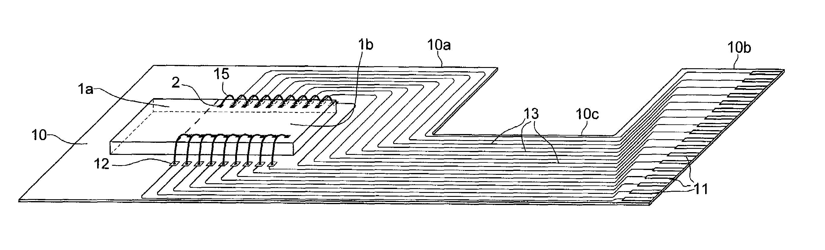
[0033]FIG. 3 shows a three-dimensional view of an optoelectronic component. On a first face of a substrate 10, which may preferably be flexible, this optoelectronic component includes an integrated photoreceptor circuit able to pick up the light generated, for example, by a light source that is not shown. The photoreceptor circuit thus includes a photosensitive area la and a processing unit area 1b in accordance with the embodiment described with reference to FIG. 1a for example.

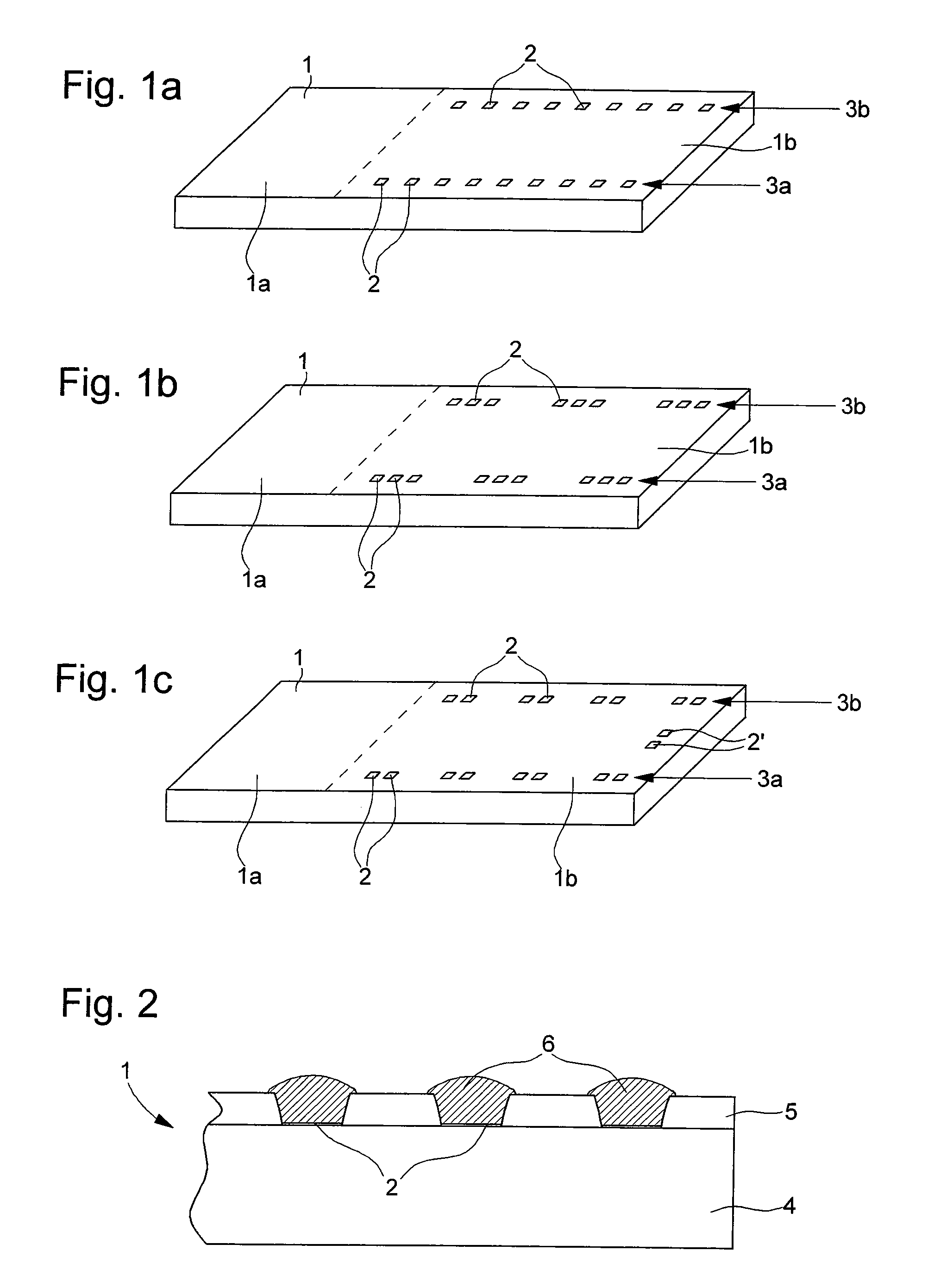
[0034]This photoreceptor circuit is mounted on a first portion 10a of flexible substrate 10 by a flip chip technique. In order to do this, contact pads 2 of the photoreceptor circuit, which include metal bumps as shown in FIG. 2, are electrically connected across corresponding connection pads 12 of the first portion of substrate 10. The connection pads are arranged in the same arrangement and position as the metal bumps of processing unit area 1b of the circuit in two rows.

[0035]The electrical connection bet...

second embodiment

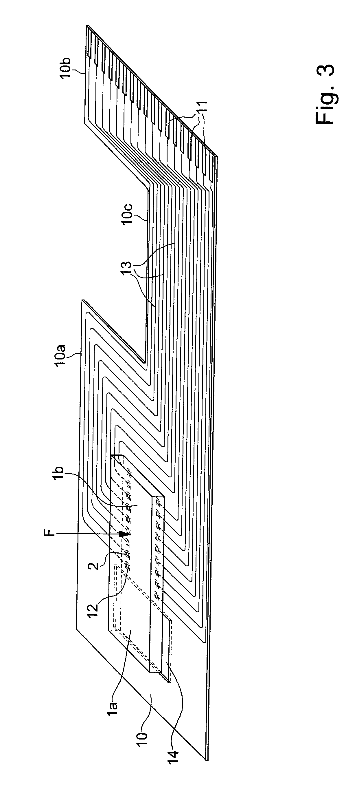
[0040]The first portion 10a of substrate 10 includes two rows of connection pads 12 each arranged on two opposite sides of processing unit area 1 only. These connection pads 12 could be arranged in the same way as contact pads 2 of processing unit area 1b. The electric connection of contact pads 2 is achieved in this second embodiment by metal wires 15, such as aluminium wires, to the corresponding connection pads 12 of first portion 10a of substrate 10. These connection pads 12 are connected to preferably metal conductive paths 13, which are arranged on one or other face of the substrate. The conductive paths thus connect connection pads 12 to connection terminals 11 placed on the second portion 10b of the substrate.

[0041]As previously, one could envisage encapsulating only the photosensitive area, either by resin, or by an opaque insulating cover that is not shown. This leaves photosensitive area 1a free without any mechanical stress during the entire method for making the optoele...


PUM


Abstract

The integrated photoreceptor circuit includes a photosensitive area for picking up light and a processing unit area for processing the signals provided by the photosensitive area. This photoreceptor circuit includes electric contact pads, which are arranged symmetrically solely on the side of the processing unit area, which is juxtaposed with the photosensitive area. The integrated photoreceptor circuit is mounted on a first portion of a flexible substrate. The contact pads of the integrated photoreceptor circuit are electrically connected to electrical connection pads of the printed circuit of the flexible substrate. A second portion of the flexible substrate carries electrical connection terminals, which are connected to the connection pads via conductive paths, arranged in part on a connecting portion between the first and second portions. A through aperture in the first portion may be provided opposite the photosensitive area only of the photoreceptor circuit.

Description

[0001]This application claims priority from Swiss Patent Application No. 00451 / 07 filed Mar. 21, 2007, the entire disclosure of which is incorporated herein by reference.FIELD OF THE INVENTION[0002]The invention concerns an integrated photoreceptor circuit, which includes a photosensitive area for picking up light and a processing unit area for processing the signals provided by the photosensitive area.[0003]The invention also concerns an optoelectronic component, which includes the integrated photoreceptor circuit.BACKGROUND OF THE INVENTION[0004]An integrated photoreceptor circuit can generally be made in a silicon semiconductor substrate. The photosensitive area of the photoreceptor circuit can include an array or matrix of photosensitive elements, such as photodiodes, or a particular configuration of several adjacent photosensitive elements. The processing unit of the photoreceptor circuit processes the signals supplied by the elements of the photosensitive area, while taking ac...

Claims


Application Information

Patent Timeline
Patent Type & Authority Patents(United States)
IPC IPC(8): H01J40/14
CPCH01L27/14636H01L31/022408H01L27/1446H01L27/14618H01L27/14634H01L2224/45124H01L2224/48227H01L2224/48091H01L2924/00014H01L2924/00
Inventor QUERCIA, VICTORIOGRANDJEAN, ANDREKAYAL, ABDUL-HAMID
Owner EM MICROELECTRONIC-MARIN
Why Eureka
Try Eureka