
Semiconductor imaging device having a plurality of pixels arranged in a matrix-like pattern

a technology of matrix-like pattern and imaging device, which is applied in the direction of radio frequency controlled devices, instruments, television systems, etc., can solve the problems that the b>4/b>tr-aps cannot be sufficiently downsized/miniaturized, and the conventional art has serious problems, etc., to suppress the variation of signal voltage, high reliability, and high precision of reading operation

Inactive Publication Date: 2009-07-14
FUJITSU SEMICON LTD
View PDF7 Cites 3 Cited by
  • Summary
  • Abstract
  • Description
  • Claims
  • Application Information

AI Technical Summary

Benefits of technology

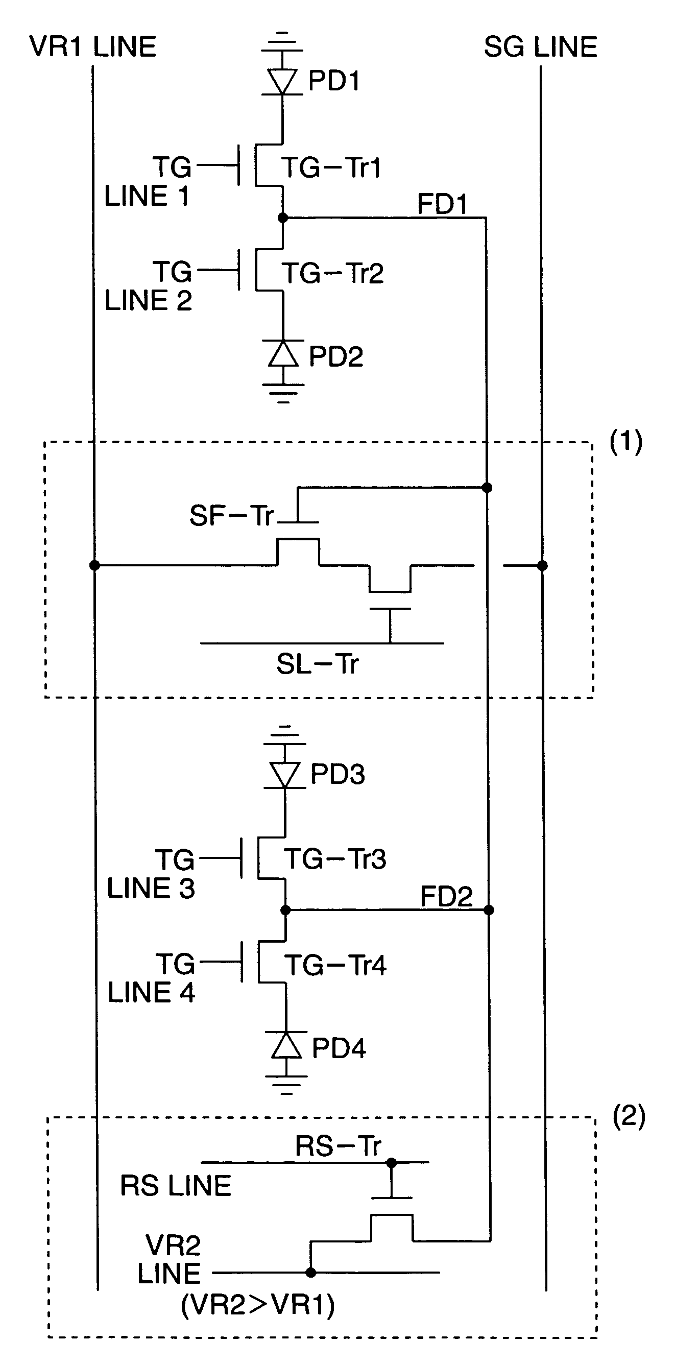
[0019]It is an object of the present invention, contrived in view of the above-mentioned problems, to provide a compact and highly reliable semiconductor imaging device, with the device intended to be downsized / miniaturized by employing an arrangement for sharing the signal voltage reading unit between four photoelectric conversion units, while realizing a highly precise reading operation by disposing respective photoelectric conversion units at intervals as even as possible to suppress signal voltage variation.

Problems solved by technology

However, the conventional art stated above has serious problems as described below.
Therefore, in this case, the 4Tr-APS cannot be sufficiently downsized / miniaturized.
However, in the case of Patent Document 2, sufficient downsizing cannot be achieved, in the first place, according to the technique for sharing the signal voltage reading unit between two PDs along the column direction.
In this case, respective PDs may have different light receiving conditions, making correct imaging operation difficult.
In addition, a problem arises in that signal voltage variation may occur because the signal voltage reading unit is disposed between adjacent PDs and necessarily, the area to be occupied by the signal voltage reading unit must be reduced.

Method used


Image

  • Semiconductor imaging device having a plurality of pixels arranged in a matrix-like pattern
  • Semiconductor imaging device having a plurality of pixels arranged in a matrix-like pattern
  • Semiconductor imaging device having a plurality of pixels arranged in a matrix-like pattern

Examples


first embodiment

[0054](Overall Arrangement of the CMOS Image Sensor)

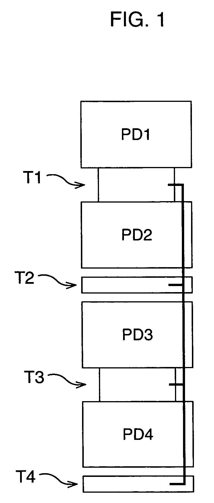
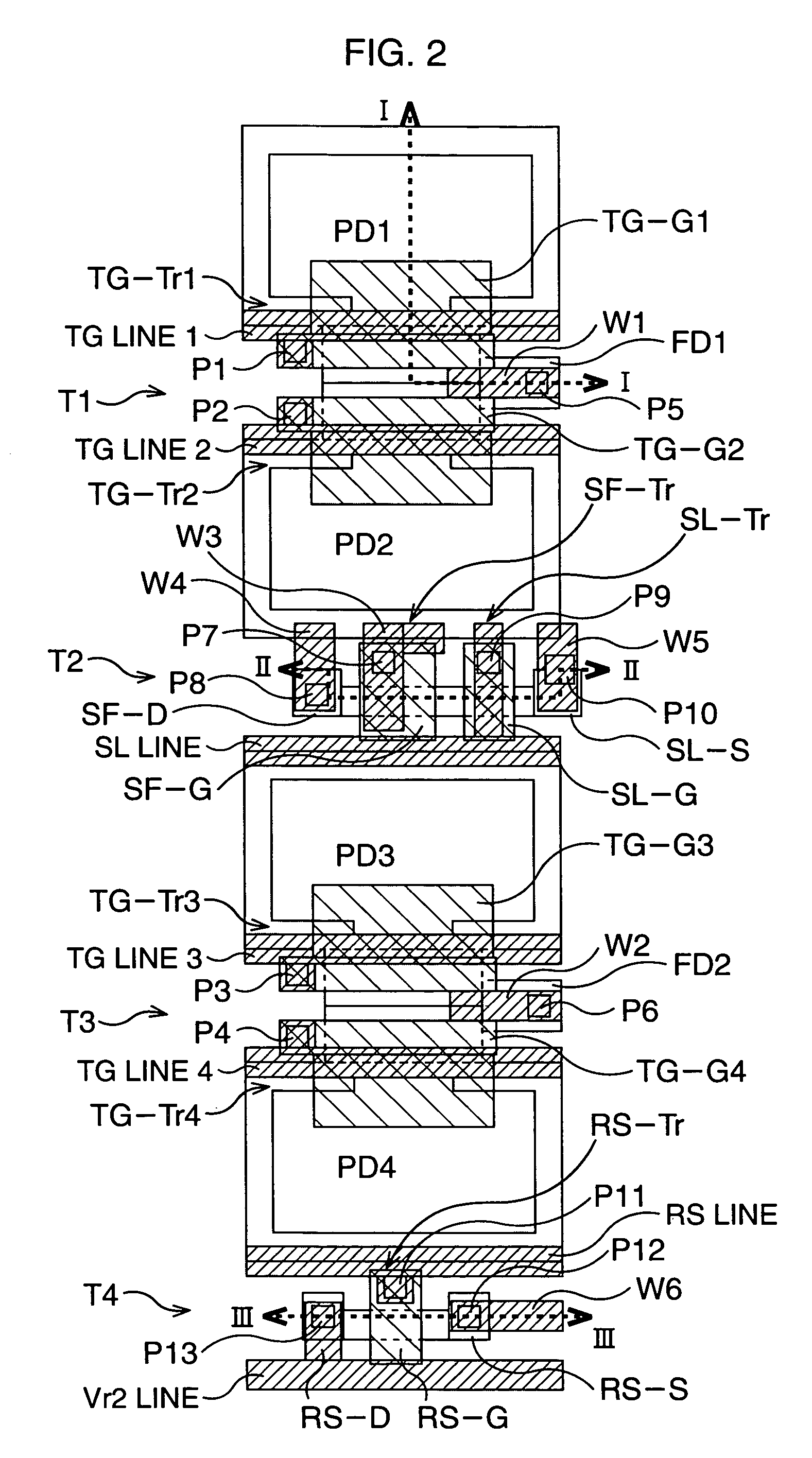
[0055]FIG. 1 is a schematic view illustrating the basic structure of the CMOS image sensor (a sensor unit including four PDs aligned along the column direction: simply referred to as a sensor unit hereafter) according to the first embodiment. FIG. 2 is a schematic plan view illustrating, in detail, the arrangement of the sensor unit of FIG. 1. FIG. 3 is a schematic view illustrating two sensor units, and FIG. 4 is a schematic plan view illustrating, in detail, the arrangement of four sensor units (inside of the dashed line corresponds to a single sensor unit). Here, FIGS. 2 and 4, illustrate, as the basic structure of the sensor unit, how a first level wiring layer is formed on the gate electrode of respective transistors.

[0056]As shown in FIGS. 1 and 2, the basic structure of the sensor unit of the present embodiment is composed of photodiodes PD1 to PD4 disposed in alignment along the column direction, a transistor structure T1 d...


PUM


Abstract

In an arrangement with four PDs (PD1 to PD4) aligned along the column direction sharing the signal voltage reading unit, respective elements are disposed in the order of: PD / FD1 and TG-Tr1,2 / PD2 / SF-Tr and SL-Tr / PD3 / FD2 and TG-Tr3, 4 / PD4 / RS-Tr.

Description

CROSS-REFERENCE TO RELATED APPLICATIONS[0001]This application is based upon and claims the benefit of priority from the prior Japanese Patent Application No. 2005-378115, filed on Dec. 28, 2005, the entire contents of which are incorporated herein by reference.BACKGROUND OF THE INVENTION[0002]1. Field of the Invention[0003]The present invention relates to a semiconductor imaging device having a plurality of pixels arranged in a matrix-like pattern.[0004]2. Description of the Related Art[0005]Generally, semiconductor imaging elements are classified broadly into CCD image sensors and CMOS image sensors. As one type of CMOS image sensors, there exists a 4Tr+1PD type 4Tr-APS (Active Pixel Sensor) including four transistors and one photodiode (PD) which form a single pixel.[0006]The structure of a pixel composing the 4Tr-APS is shown in FIGS. 24A and 24B.[0007]In the 4Tr-APS, as shown in FIG. 24A, a photodiode (PD) photoelectrically converts the received light by means of NP junction and...

Claims


Application Information

Patent Timeline
Patent Type & Authority Patents(United States)
IPC IPC(8): H01L27/00H04N3/14H01L27/146
CPCH01L27/14603H01L27/14641H01L27/14609
Inventor OHKAWA, NARUMI
Owner FUJITSU SEMICON LTD
Learn More