Eureka AIR delivers breakthrough ideas for toughest innovation challenges, trusted by R&D personnel around the world.

Drop-in heat sink and exposed die-back for molded flip die package

a technology of drop-in heat sink and flip-type package, which is applied in the direction of semiconductor devices, semiconductor/solid-state device details, electrical equipment, etc., can solve the problems of not being able to efficiently dissipate heat, generating additional heat, and not being as good a thermal conductor as ceramics

Active Publication Date: 2009-07-14
MARVELL ASIA PTE LTD
View PDF23 Cites 7 Cited by
  • Summary
  • Abstract
  • Description
  • Claims
  • Application Information

AI Technical Summary

Benefits of technology

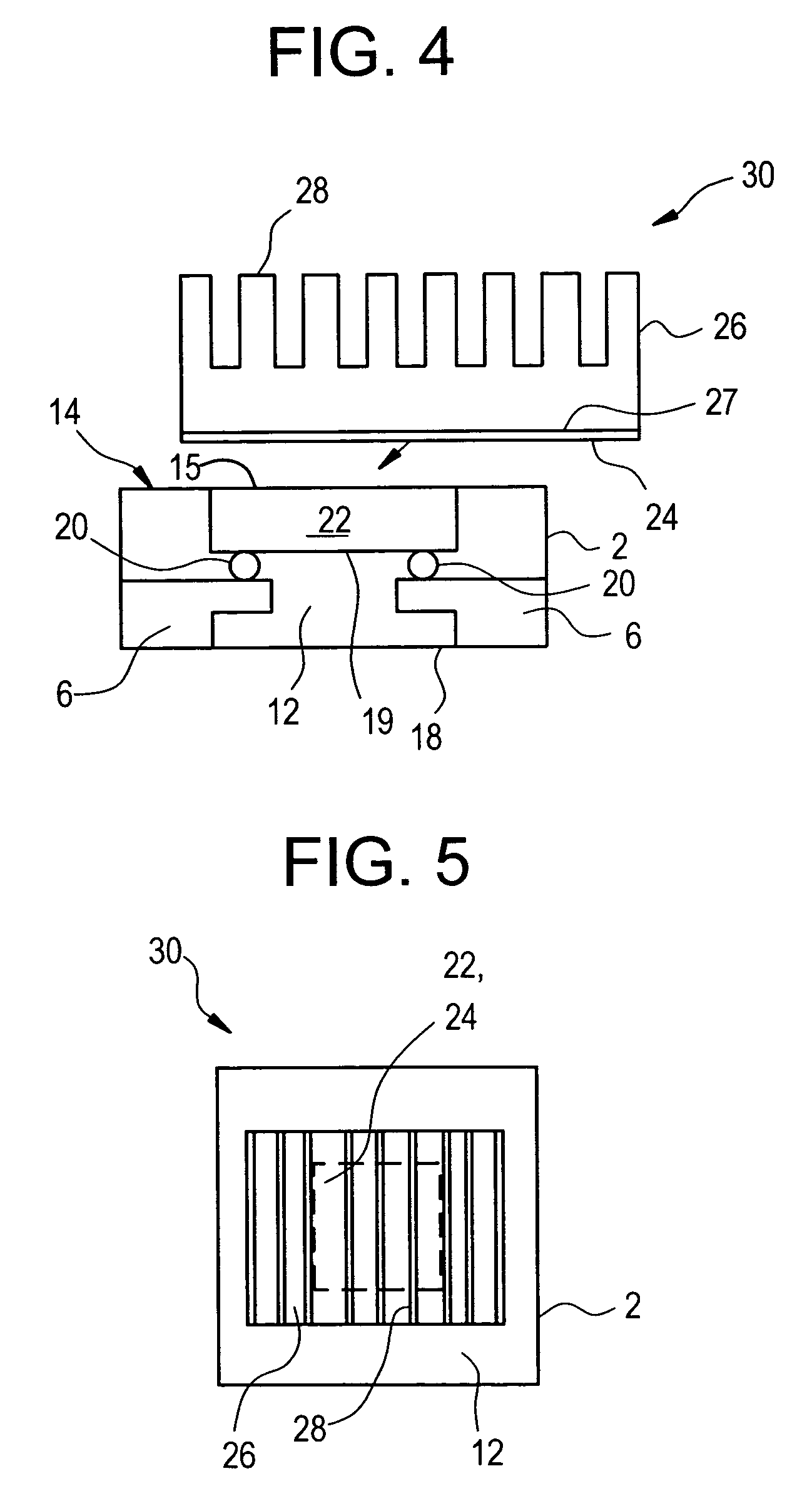
[0012]According to the first aspect, the step of providing the molded IC flip die encapsulated with molding material comprises the step of: (d) providing the molded IC flip die comprising a first surface, portions of which are in electrical contact with one or more lead pads, and a second surface opposed to the first surface. The step of exposing the surface of the integrated circuit die in the molded IC flip die package comprises: (e) selectively removing a portion of the molding material to expose the second surface of the integrated circuit die. The step of selectively removing a portion of the molding material to expose the second surface of the integrated circuit die comprises: (f) abrading the molding material to selectively remove a portion of the molding material to expose the second surface of the integrated circuit die. The step of abrading the molding material comprises: (g) abrading the molding material initially with a coarse grit abrasion material; (h) and abrading the molding material subsequently with a finer grit abrasion material to selectively remove a portion of the molding material to expose the second surface of the integrated circuit die. The step of selectively removing the portion of the molding material to expose the second surface of the integrated circuit die comprises: (i) selectively removing the portion of the molding material with a removing apparatus selected from the group consisting of a laser, a drill, and one or more chemicals to expose the first surface of the integrated circuit die. The step of selectively removing the portion of the molding material with a laser comprises: (j) ablating the portion of molding material with a laser. The step of selectively removing the portion of the molding material with a laser comprises: (k) shearing off the portion of molding material with a laser. The step of selectively removing a portion of the molding material with one or more chemicals comprises: (l) removably etching the portion of molding material with one or more chemicals.

Problems solved by technology

However, as circuit densities increase, semiconductor die generate additional heat, and the leads of the package are not always able to efficiently dissipate the heat.
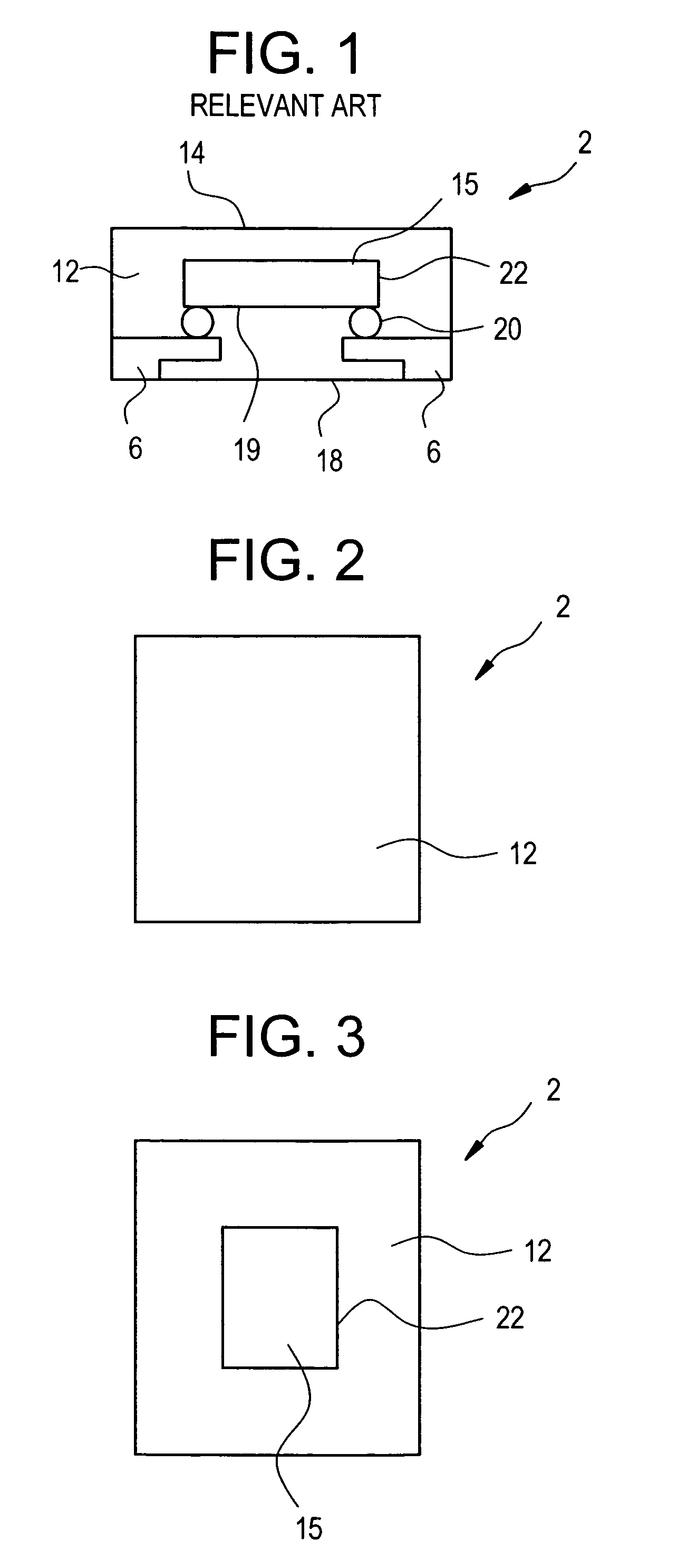
Plastic, however, is not as good a thermal conductor as ceramic, and MFD ICs 2 (and other types as well) can be required to dissipate 5, 10 or even up to 20 watts of power.

Method used


Image

  • Drop-in heat sink and exposed die-back for molded flip die package
  • Drop-in heat sink and exposed die-back for molded flip die package
  • Drop-in heat sink and exposed die-back for molded flip die package

Examples


second embodiment

[0065]FIG. 10 illustrates a flow chart of a method 200 to attach a heat sink 26 to a die 22 in a MFD IC 2 according to the present invention. The method 200 represents a first method for creating the second MFD IC heat sink assembly 32. The method 200 begins with step 202 wherein the MFD IC 2 is manufactured according to a conventional manufacturing process (or provided to the user of method 200), except that molding material 12 is not yet added to encapsulate the assembled MFD IC 2. Then, in step 204, the heat sink 26 is attached to the die 22, using any appropriate means for attaching the heat sink 26 to the die 22, such as those discussed previously. Following the attachment of the heat sink 26 to the 22, the assembled heat sink 26 and 22 are encapsulated with the molding material 12 in step 206.

[0066]FIGS. 11-13 illustrate a MFD IC 2 that is assembled according to an alternative embodiment of the present invention. In FIG. 11, a MFD IC 2 that has been manufactured in the convent...

third embodiment

[0071]FIG. 17 illustrates a flow chart of a method 300 to attach a heat sink 26 to a die 22 in a MFD IC 2 according to the present invention. The method 300 represents a first method for creating the third MFD IC heat sink assembly 34. The method 300 begins with step 302 wherein the MFD IC 2 is manufactured according to a conventional manufacturing process (or provided to a user of method 300), except that molding material 12 is not yet added to encapsulate the assembled MFD IC 2. Then, in step 304, the heat sink 26 is attached to the die 22, using any suitable means for attaching the heat sink 26 to the die 22, such as those discussed above. Following the attachment of the heat sink 26 to the die 22, the assembled heat sink 26 and die 22 are encapsulated with the molding material 12 in step 306.

[0072]FIG. 18 illustrates a bottom view of a MFD IC 2 encapsulated by a molding material, then modified according to an embodiment of the present invention. FIG. 19 illustrates a bottom view...


PUM


Abstract

A system and method for modifying a molded flip die (MFD) integrated circuit package that includes an integrated circuit die to include a heat sink such that the heat sink is thermally coupled to either a top or bottom portion of the integrated circuit die and can then dissipate heat to ambient air. The system and method presented herein modify the MFD package by either removing portions of a molding material and attaching the heat sink directly to the die, or thermally coupling the heat sink to the die prior encapsulation of the integrated circuit die and heat sink.

Description

BACKGROUND[0001]1. Field of the Invention[0002]The present invention relates to a system and method for dissipating excess heat from integrated circuit semiconductors. More particularly, the present invention relates to a system and method for dissipating excess heat through the use of externally and internally located heat sinks for molded flip die (MFD) packaged integrated circuits.[0003]2. Background Information[0004]An integrated circuit (IC) package is a structure used to electrically connect an IC die (die) to a printed circuit board (PCB) or other host structure. Each die typically includes input / output (I / O) terminals which are arranged along a peripheral edge of the die. After the die is mounted on a package, the I / O terminals are electrically connected to bonding pads formed on the package using, for example, wire bond techniques.[0005]In order to maintain a reasonable service life of an IC device, the operating temperature of the device must be carefully controlled by pro...

Claims


Application Information

Patent Timeline
IPC IPC(8): H01L21/00
CPCH01L23/36H01L23/4334H01L23/49548H01L23/3107H01L2924/01019H01L2224/73253H01L2224/16245H01L21/568H01L2224/32245H01L2224/73203
Inventor KAO, HUAHUNGLIOU, SHIANN-MING
Owner MARVELL ASIA PTE LTD
Why Eureka
Eureka Blog
Learn More