
Programmable logic device with on-chip nonvolatile user memory

a programmable logic and user memory technology, applied in the field of integrated circuits, can solve the problems of more devices taking more time and more complex test equipment, and achieve the effect of reducing the complexity of the board design and saving time and test equipment resources

Active Publication Date: 2009-06-23
TAHOE RES LTD
View PDF6 Cites 53 Cited by
  • Summary
  • Abstract
  • Description
  • Claims
  • Application Information

AI Technical Summary

Benefits of technology

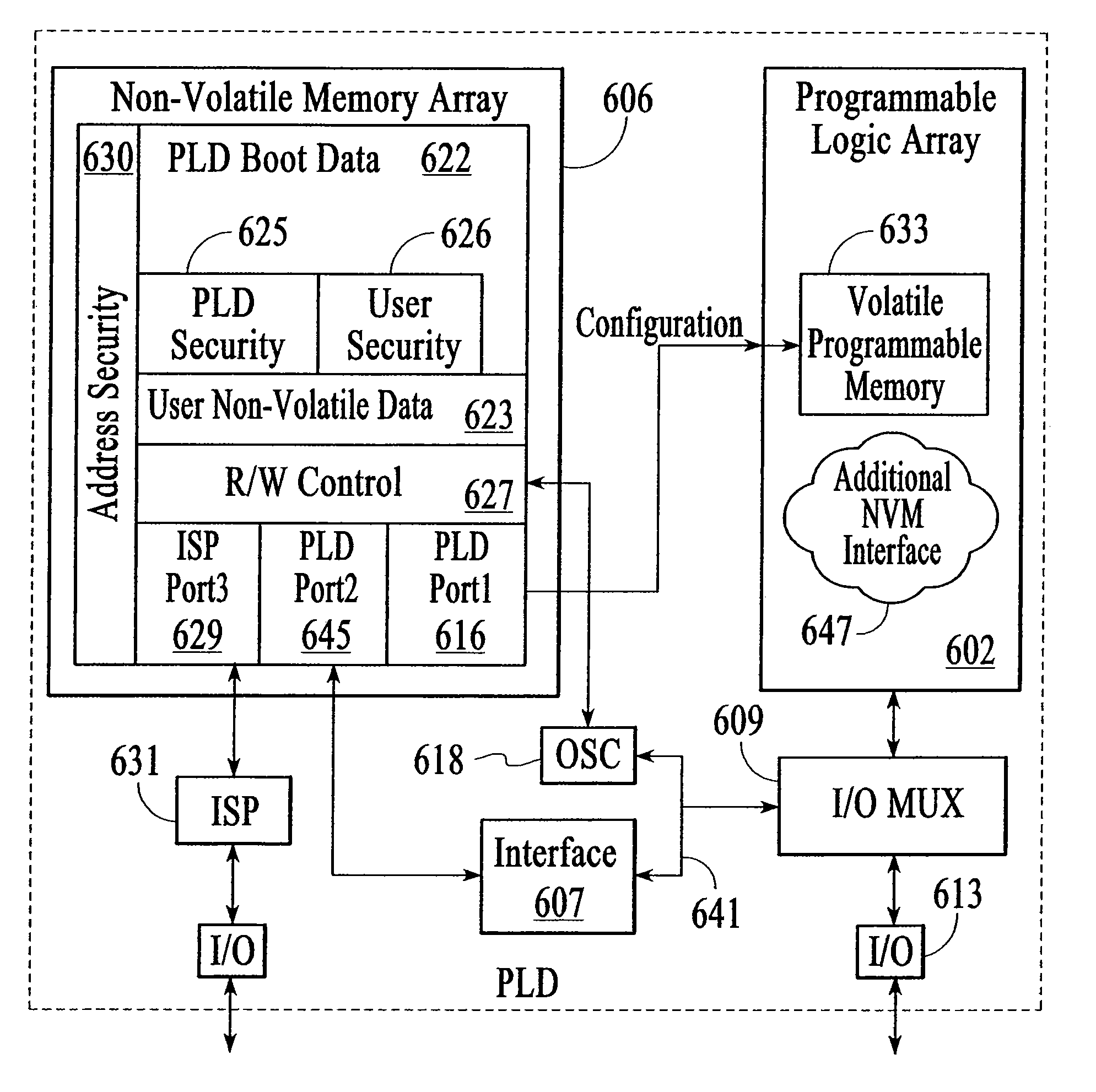
The invention is a programmable logic integrated circuit with a nonvolatile memory that allows users to store and retrieve data. This embedded memory reduces the complexity of board designs and saves time and test equipment in manufacturing. The nonvolatile memory includes a boot data partition for configuring the programmable logic and a user data partition for storing user data. The programmable logic device can access the user data through an interface block connected to the nonvolatile memory. The technical effects of this invention include simplifying board designs, saving manufacturing resources, and improving operational efficiency.

Problems solved by technology

More devices take more time and more complex test equipment.

Method used


Image

  • Programmable logic device with on-chip nonvolatile user memory
  • Programmable logic device with on-chip nonvolatile user memory
  • Programmable logic device with on-chip nonvolatile user memory

Examples


Embodiment Construction

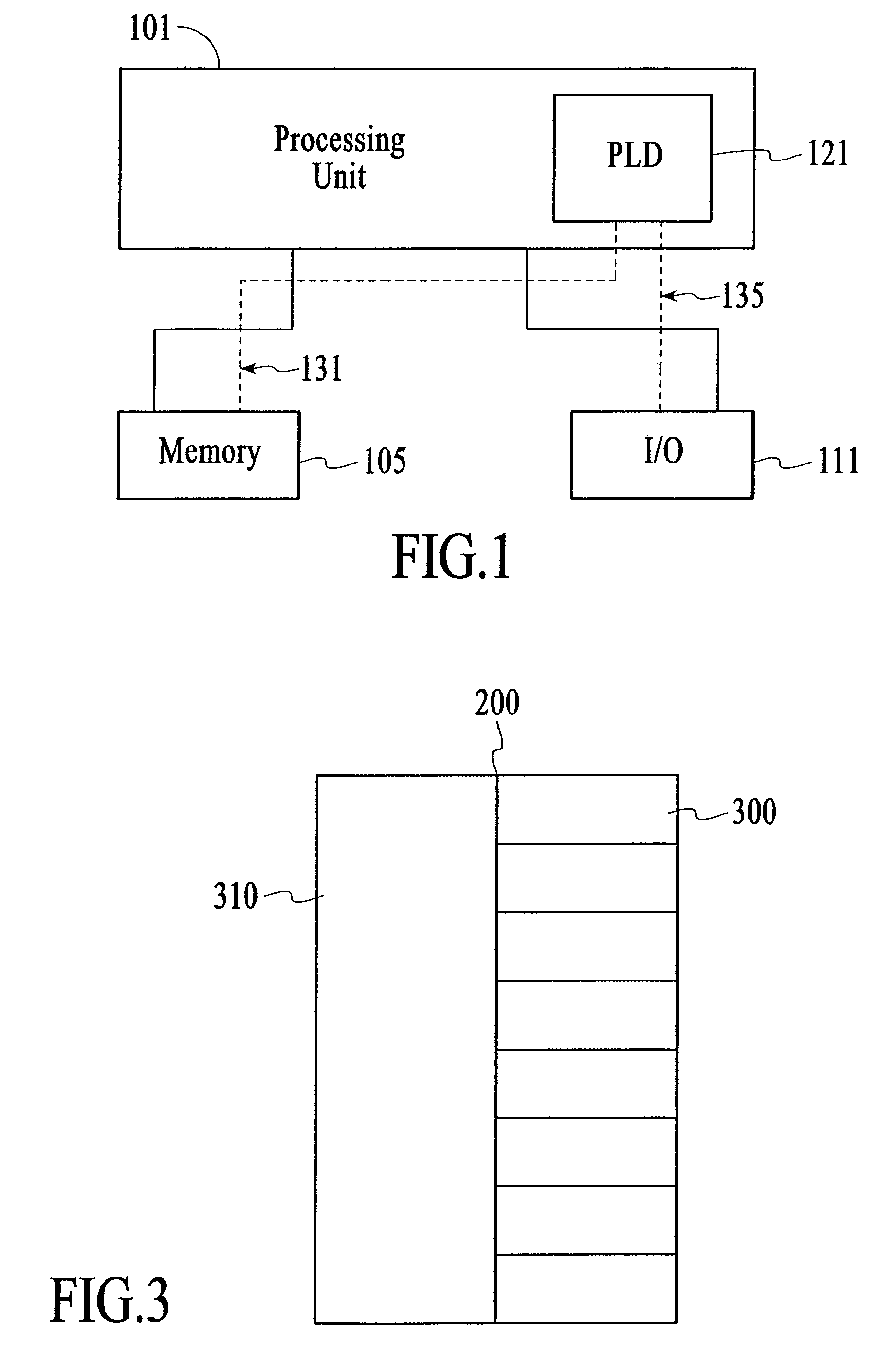
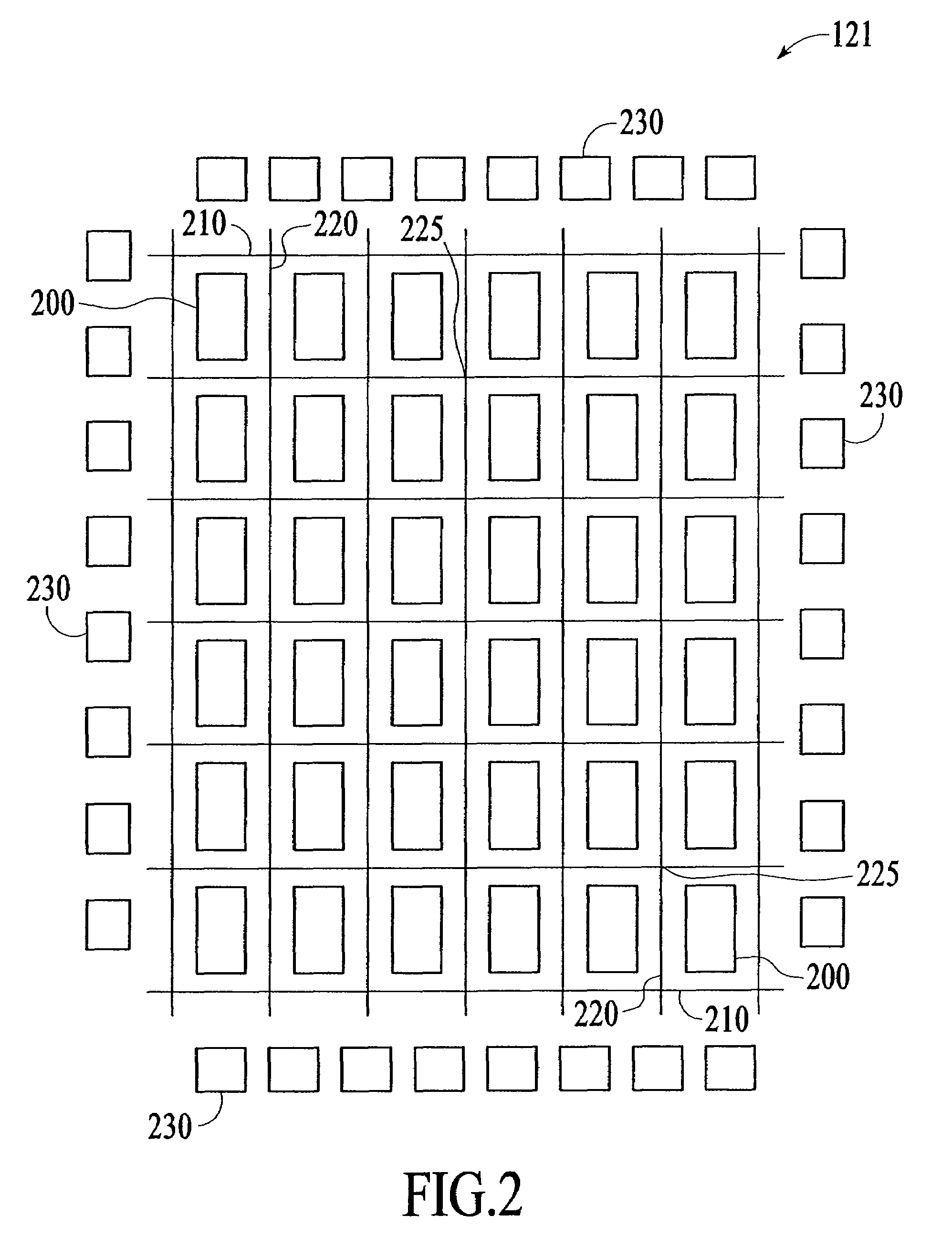
[0022]FIG. 1 shows a block diagram of a digital system, within which input and output interfaces consistent with the present invention may be embodied. The system may be provided on a single board, on multiple boards, or within multiple enclosures. Though embodiments of the present invention are useful in electronic and integrated circuits in general, they are particularly useful in programmable logic devices. FIG. 1 illustrates a system 101 in which such a programmable logic device 121 may be utilized. Programmable logic devices or programmable logic integrated circuits are sometimes referred to as a PALs, PLAs, FPLAs, PLDs, CPLDs, EPLDs, EEPLDs, LCAs, or FPGAs and are well-known integrated circuits that provide the advantages of fixed integrated circuits with the flexibility of custom integrated circuits. Such devices allow a user to electrically program standard, off-the-shelf logic elements to meet a user's specific needs. Examples of current programmable logic devices are repre...


PUM


Abstract

A programmable logic integrated circuit has user-accessible nonvolatile memory for use by the programmable logic. In a specific embodiment, the programmable logic integrated circuit has a programmable logic array portion and a nonvolatile memory array portion. The nonvolatile memory array portion is segregated into a boot data part and a user data partition. The boot data partition holds data for configuring the programmable logic portion on power up, and the user data partition is for use by the programmable logic. A user can store and retrieve data from the user data partition. A built-in oscillator can be programmably connected from the nonvolatile memory portion to the PLD portion.

Description

CROSS-REFERENCES TO RELATED APPLICATIONS[0001]This application is a continuation of U.S. patent application Ser. No. 10 / 754,432, filed Jan. 9, 2004, the disclosure of which is incorporated herein by reference.BACKGROUND OF THE INVENTION[0002]The present invention relates to the field of integrated circuits and in particular, to a integrated circuit having a programmable logic array portion with volatile configuration memory and a nonvolatile memory array portion.[0003]Integrated circuits are important building blocks of the modern age. Technology continues to evolve and integrated circuits continue to provide improved functionality. As integrated circuits improve, so do the electronics systems that are built using integrated circuits. There are many types of integrated circuit such as memories, microprocessors, application specific integrated circuits (ASICs), and programmable logic. Programmable logic integrated circuits such as PALs, PLDs, FPGAs, LCAs, and others are becoming more...

Claims


Application Information

Patent Timeline
Patent Type & Authority Patents(United States)
IPC IPC(8): G06F7/38H03K19/173
CPCG11C7/20H03K19/1776H03K19/17772
Inventor CAMAROTA, RAFAEL C.WHITE, THOMAS H.
Owner TAHOE RES LTD
Learn More