LED chip packaging structure

a technology of packaging structure and led chip, which is applied in the direction of basic electric elements, electrical equipment, semiconductor devices, etc., can solve the problems of inextricable heat dispersing problem, poor heat dispersing effect, and high cost of gold wire bonds, and achieves improved heat dispersal effect, low cost, and increased packaging efficiency

Inactive Publication Date: 2009-05-12
RODMAN ELECTRONICS
View PDF1 Cites 2 Cited by
  • Summary
  • Abstract
  • Description
  • Claims
  • Application Information

AI Technical Summary

Benefits of technology

[0009]To overcome the aforementioned shortcomings of the prior arts, the object of the present invention is to provide an improved LED chip packaging structure, the cost of which is lowered, the heat dispersal effect is improved, the packaging efficiency is increased, and the market competition is enhanced.
[0015]By the aforementioned technology, the present invention can overcome the shortcomings of the prior arts and has the advantageous of low cost, the heat dispersal effect is improved, the packaging efficiency is increased, and the market competition is enhanced.

Problems solved by technology

However, the high operating current of the new high power LEDs leads to an inextricable heat dispersing problem.
Thus, the heat dispersing effect is bad.
Moreover, the conducting wires 14 of the aforementioned LED chip packaging structure 1 is bonded by a gold wire bond, but gold wire bonds are expensive, so the users are overburdened for the high cost.
Furthermore, the drying processes of the phosphor 151 and the silica gel 152 lead to low efficiency and high cost.
However, such structure must be used in the double substrates, which is also high-cost, and the manufacture efficiency cannot be increased.

Method used


Image

  • LED chip packaging structure
  • LED chip packaging structure
  • LED chip packaging structure

Examples


Embodiment Construction

[0019]The invention, in accordance with preferred and exemplary embodiments, together with further technology, means and advantages thereof, is more particularly comprehended in the following detailed description.

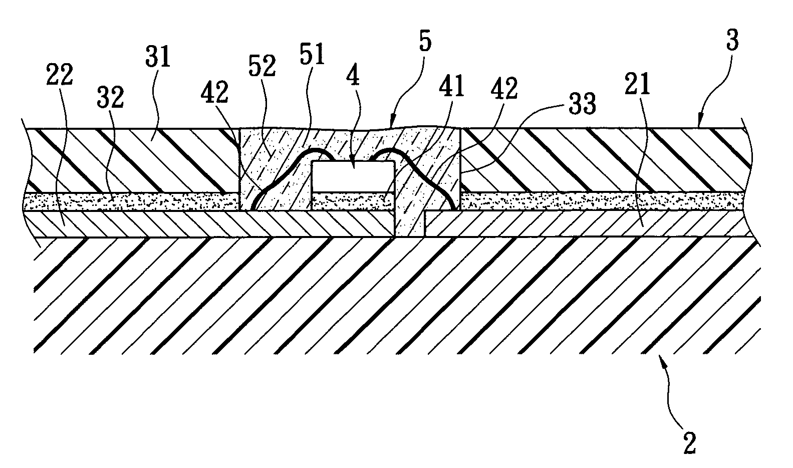
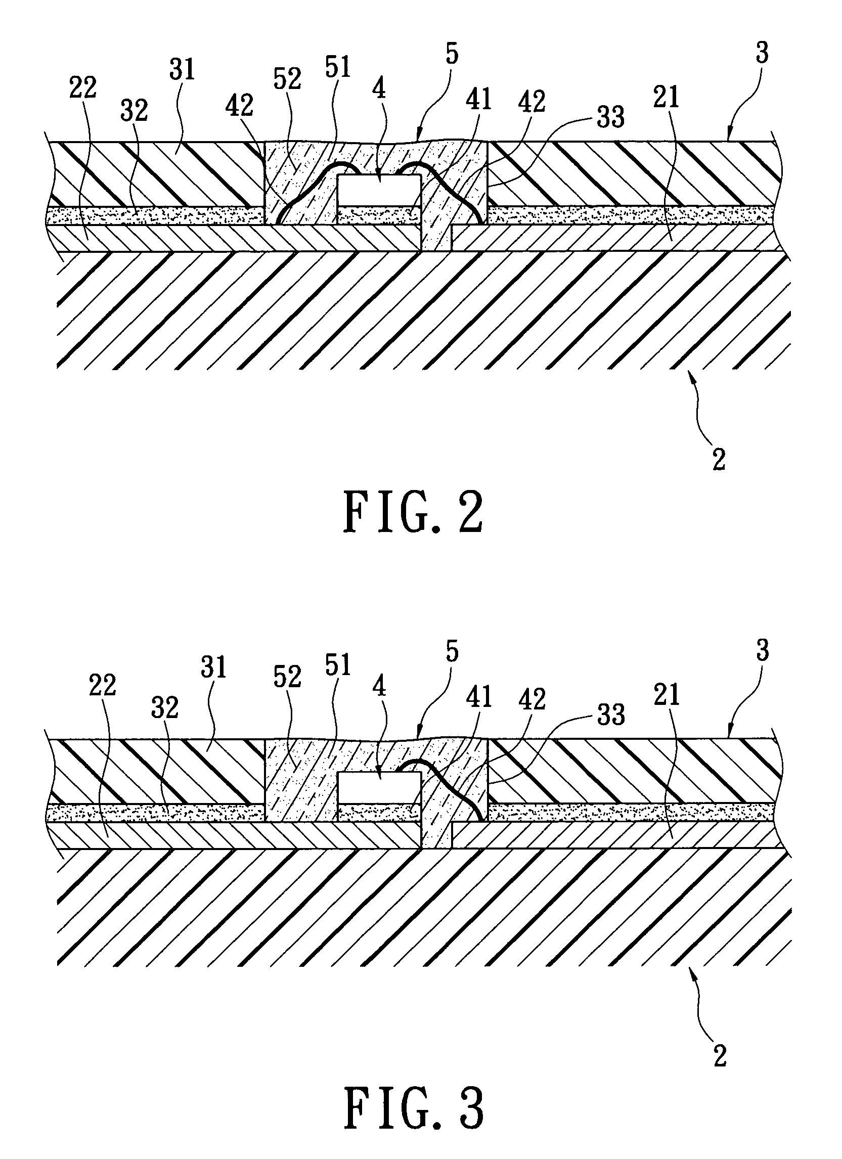
[0020]Please refer to FIG. 2 illustrating an improved LED chip packaging structure of the present invention. The structure includes a substrate 2, an insulating layer 3, a light emitting chip 4, and sealing adhesive 5.

[0021]At least two conductive traces 21, 22 are disposed on at least one side surface of the substrate 2. The conductive traces 21, 22 are respectively an anode and a cathode of an electrical source. Further, the material of the substrate 2 is copper alloy, aluminum alloy, ceramics, or their combination.

[0022]The insulating layer 3 attaches on one side surface of the substrate 2 fitted with the conductive traces 21, 22. The insulating layer 3 includes an insulating film 31, an agglutinating layer 32 is adhered between the insulating film 31 and the substrate 2...


PUM


Abstract

An improved LED chip packaging structure includes a substrate, an insulating layer, a light emitting chip and sealing adhesive. At least two conductive traces are disposed on at least one side surface of the substrate. The insulating layer attaches on one side surface of the substrate and includes an insulating film. The light emitting chip is received in the through hole of the insulating layer and attaches on one side surface of the substrate. An adhesive is securing the light emitting chip on the substrate, and the light emitting chip connects with at least one conducting wire. The sealing adhesive is filled into the through hole of the insulating layer. By the direct combination of the light emitting chip and the substrate, the present invention has the advantageous of low cost, the heat dispersal effect is improved, the packaging efficiency is increased, and the market competition is enhanced.

Description

BACKGROUND OF THE INVENTION[0001]1. Field of the Invention[0002]The present invention relates to an improved LED chip packaging structure, and more particular to a structure of a light emitting chip directly integrating with a substrate, thus, the present invention has the advantages of low-cost, improved heat dispersing effect, increased packaging efficiency, and enhanced competitiveness.[0003]2. Description of Related Art[0004]Nowadays, because the illuminating power of conventional LED has been increased, LEDs can be used as not only indicating lights or assistant lights, but also illuminating lights. Moreover, the operating current of the present high power LED may be over 2 amperes, and the operating current of conventional LEDs may be only 20 milliamperes, so that the operating current of the present high power LEDs is over 100 times larger than that of conventional LEDs, namely, the illuminating power of single high power LED is higher than a hundred of conventional LEDs. Thu...

Claims


Application Information

Patent Timeline
Patent Type & Authority Patents(United States)
IPC IPC(8): H01L33/00H01L33/48H01L33/64
CPCH01L33/647H01L33/483H01L33/641H01L2224/48091H01L2224/48465H01L2224/73265H01L2924/00014H01L2224/45124H01L2224/45144H01L2924/00
Inventor HUANG, CHIH-FANGCHA, FOM-PU
Owner RODMAN ELECTRONICS
Why Eureka
Try Eureka