
Organic EL display device and method of driving the device

a display device and organic el technology, applied in static indicating devices, instruments, electroluminescent light sources, etc., can solve the problems of increasing power consumption, reducing the efficiency of electric current supply of insufficient charge supply to be lit by organic el light emitting elements to achieve the effect of enhancing brightness, reducing power consumption, and effective supply

Active Publication Date: 2009-04-14
SHARP KK
View PDF14 Cites 0 Cited by
  • Summary
  • Abstract
  • Description
  • Claims
  • Application Information

AI Technical Summary

Benefits of technology

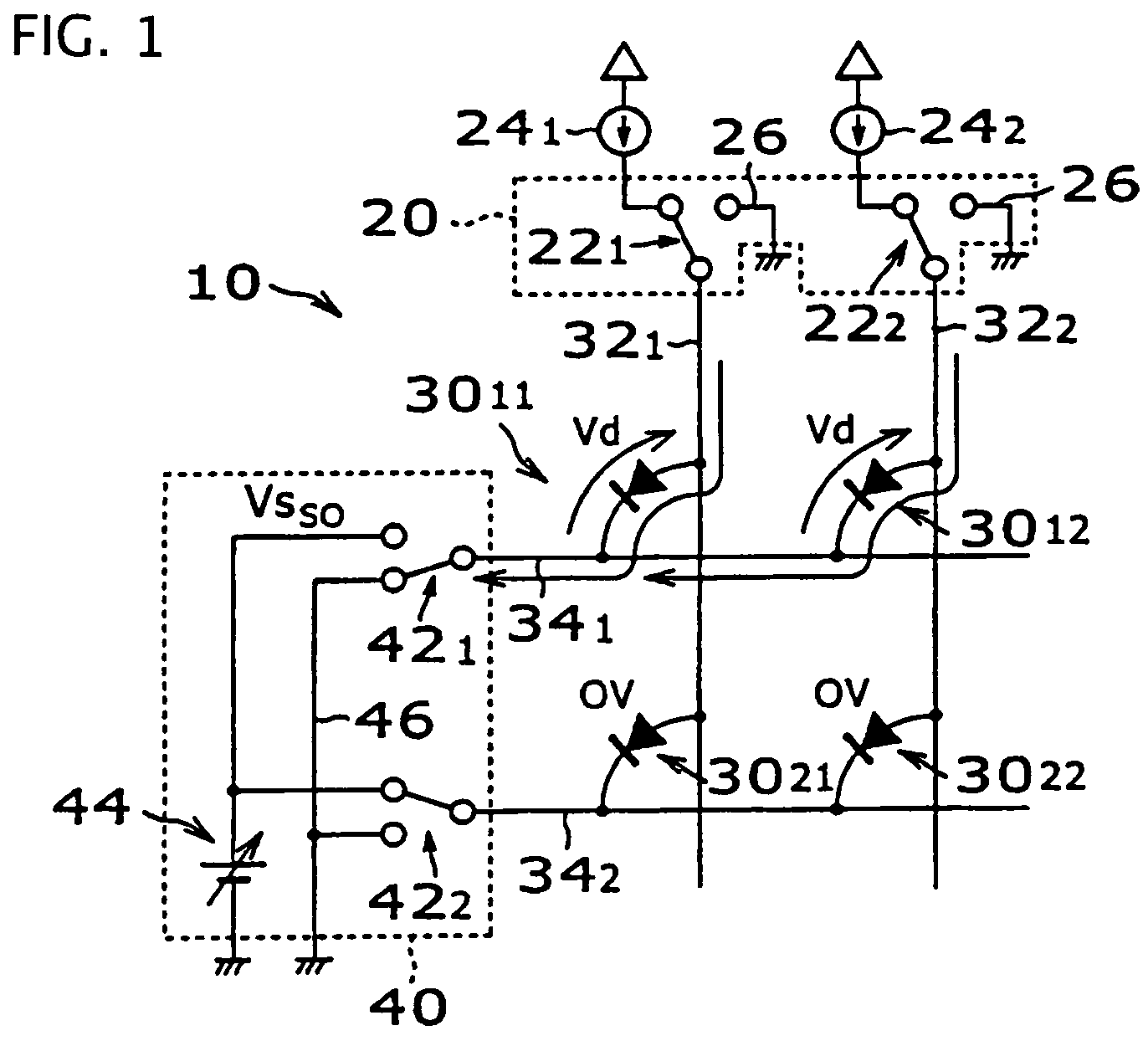
The present invention provides an organic EL display device and an operation method that reduces power consumption and enhances brightness of the lighting pixels. This is achieved by reducing input of charges into unselected pixels and selectively connecting the second electrode elements to either a power supply or ground based on the display pattern. The second power supply is synchronized with the first driving unit to change its voltage in synchronization with the output of the light emitting current from the first driving unit. This reduces the amount of charges in unselected pixels and effectively supplies charges to the lighting pixels, resulting in enhanced brightness and reduced power consumption in a passive matrix type organic EL display device.

Problems solved by technology

As a result, a problem arises that sufficient charges cannot be supplied to the organic EL light emitting element to be lighted.
The organic EL light emitting element suffers degradation in electric current efficiency, an increase in power consumption, and a shortening of operation life.
In addition, the power loss due to charging and discharging on every switching of selected scanning electrode element cannot be ignored.
In the method of cathode reset, however, a large inrush current flows into the lighting organic EL light emitting element from the unselected scanning electrode elements all at once, which raises the problem of a heavy load on the driver IC.

Method used


Image

  • Organic EL display device and method of driving the device
  • Organic EL display device and method of driving the device
  • Organic EL display device and method of driving the device

Examples


first aspect of embodiment

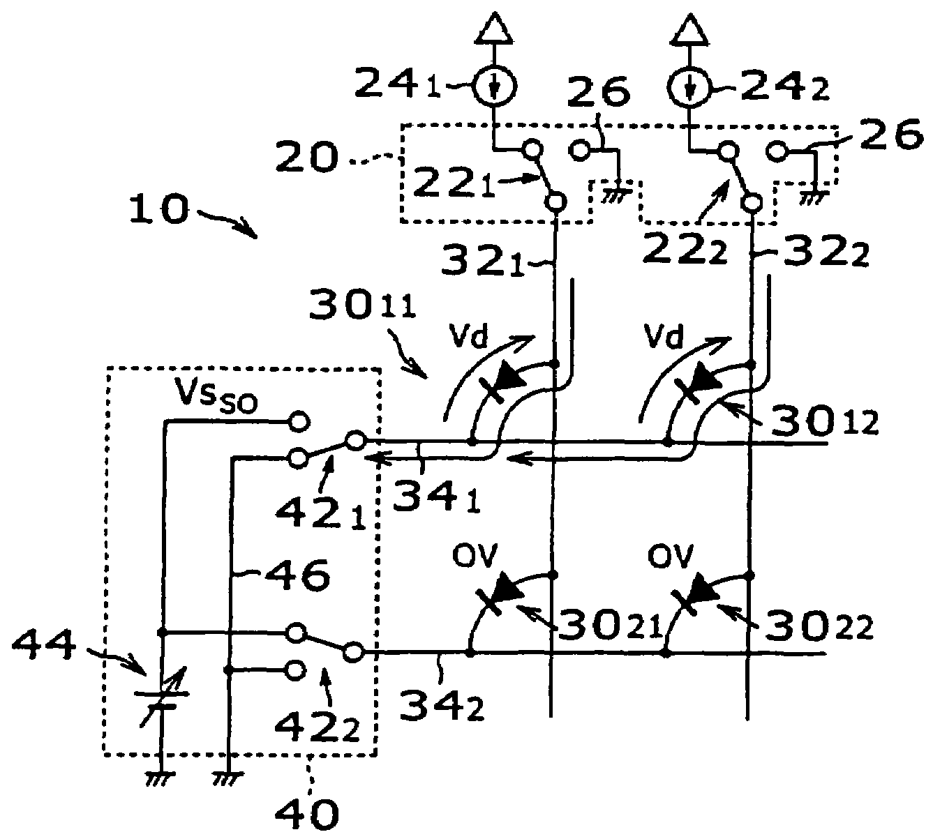
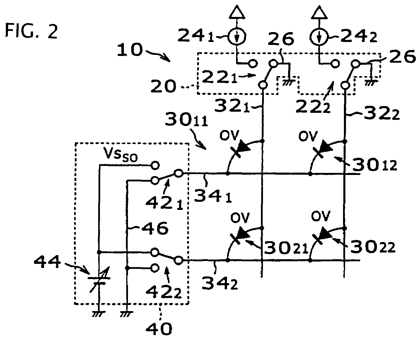
[0032]FIGS. 1 through 4 are circuit diagrams showing a part of organic EL display device 10 of an embodiment according to the invention. The figures show the current through pixels and the voltage across pixels when a scanning electrode element is selected and switched to another scanning electrode element. The figures illustrate operation of the organic EL display device 10 referring to 2×2 organic EL light emitting elements 3011, 3012, 3021, and 3022 composing a part of the display device. The organic EL display device are provided with data electrode elements (first electrode elements) 321 and 322, and scanning electrode elements (second electrode elements) 341 and 342. Each electrode element connects to a switching element that conducts a push-pull type operation. The operation of the switching elements is equivalently represented by switches 221, 222, 421, and 422. Switches 221 and 222 conduct switching of data electrode elements 321 and 322 between connection to display curren...

second aspect of embodiment

[0049]FIG. 6 shows a structure of an organic EL display device of another embodiment according to the invention. In this embodiment, the voltage wave form of first electrode elements that connect to the organic EL light emitting elements to be lighted is monitored to control variable voltage power supply 44, which is a second power supply.

[0050]In this embodiment, the voltage variation Vs of variable voltage power supply 44 coincides with the voltage variation Vd of display current source 24. Consequently, this embodiment is provided with control means 52 that monitors the wave form on the data electrode element connecting to the pixels to be lighted and generates control signals to control so that the voltage wave form of variable voltage power supply 44 coincides with the monitored wave form on the data electrode element. If the voltage Vs is made exactly same as the voltage Vd, the reverse bias voltage can be made to be zero volts on organic EL light emitting elements 3021 and 30...

third aspect of embodiment

[0051]FIG. 7 shows a structure of an organic EL display device of third embodiment according to the invention. In this embodiment, variable voltage power supply 44, which is a second power supply, is controlled corresponding to the current from display current source 24.

[0052]This embodiment, in the case where display current source 24 is a constant current source, utilizes the fact that the delayed rising of the voltage wave form (FIG. 5) associated with driving a load can be determined from the output current value of current source 24. Thereby, the wave form of the voltage Vs of variable voltage power supply 44 can be made to coincide with the wave form of the voltage Vd of display current source 24. Consequently, this embodiment is provided with control means 54 that generates a control signal to control the delayed rising waveform of the voltage of variable voltage power supply 44.


PUM


Abstract

An organic EL display device is disclosed that prevents charging and discharging that do not contribute to light emission, thereby reducing power consumption. The organic EL display device comprises a plurality of first electrode elements, a plurality of second electrode elements crossing the first electrode elements, and organic light emitting layers sandwiched by the first electrode elements and the second electrode elements. A first driving unit passes light emitting current through the first electrode elements. A second driving unit connects the second electrode elements to the ground to pass the light emitting current and to a second power supply not to pass the light emitting current. The voltage of the second power supply is varied in synchronism with the voltage waveform of output of the light emitting current from the first driving unit.

Description

CROSS REFERENCE TO RELATED APPLICATIONS[0001]This application is based on, and claims priority to, Japanese Application No. 2005-041670, filed on Feb. 18, 2005, the contents of which are incorporated herein by reference.BACKGROUND OF THE INVENTION[0002]A. Field of the Invention[0003]The present invention relates to an organic EL display device and a method of driving the device, in particular, to a passive matrix type organic EL display device that exhibits enhanced brightness and reduced power consumption and a method of driving such a device.[0004]B. Description of the Related Art[0005]An organic EL display device performs high visibility owing to the self light emitting nature and low voltage driving ability thereof. Accordingly, it is being actively researched for practical applications. A type of known organic EL light emitting element composing each pixel of an organic EL display device comprises an anode of a transparent conductive film formed on a transparent substrate and a...

Claims


Application Information

Patent Timeline
Patent Type & Authority Patents(United States)
IPC IPC(8): G09G3/36H05B44/00
CPCG09G3/3216G09G3/3266G09G3/3283G09G2320/0223G09G2320/0252G09G2330/021G09G3/30
Inventor ONODA, TAKATOSHI
Owner SHARP KK
Learn More