SIMD processor with exchange sort instruction operating or plural data elements simultaneously

Inactive Publication Date: 2009-03-03
RICOH KK
View PDF5 Cites 14 Cited by
  • Summary
  • Abstract
  • Description
  • Claims
  • Application Information

AI Technical Summary

Benefits of technology

[0031]It is an object of the present invention to provide a method of data sorting processing with high speed on each processor element of an SIMD microprocessor.

Problems solved by technology

Although a normal weighting filter can be used for removing noise components of input image data, such kind of weighting filter has defect that contour portions are blurred.
However, the above methods can not be applied to image processing using an SIMD type microprocessor.
However, this method slows down the processing time for an SIMD type microprocessor because that the branch processing can not be performed on PE by PE basis and all branched operations have to be done.
Further, if counters and adders for bit slices are provided for all bits of each PE, circuit size will be unrealistically increased.
This method does not disclose the basic “three pixel sort processing”, and therefore the basic “three pixel sort processing” can not be performed with satisfactorily high speed.

Method used


Image

  • SIMD processor with exchange sort instruction operating or plural data elements simultaneously
  • SIMD processor with exchange sort instruction operating or plural data elements simultaneously
  • SIMD processor with exchange sort instruction operating or plural data elements simultaneously

Examples


first embodiment

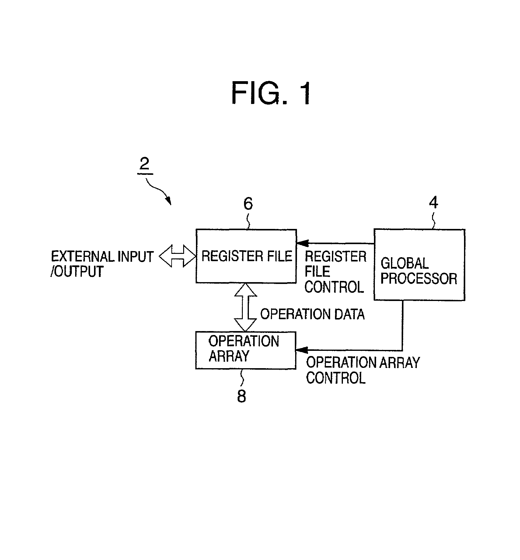
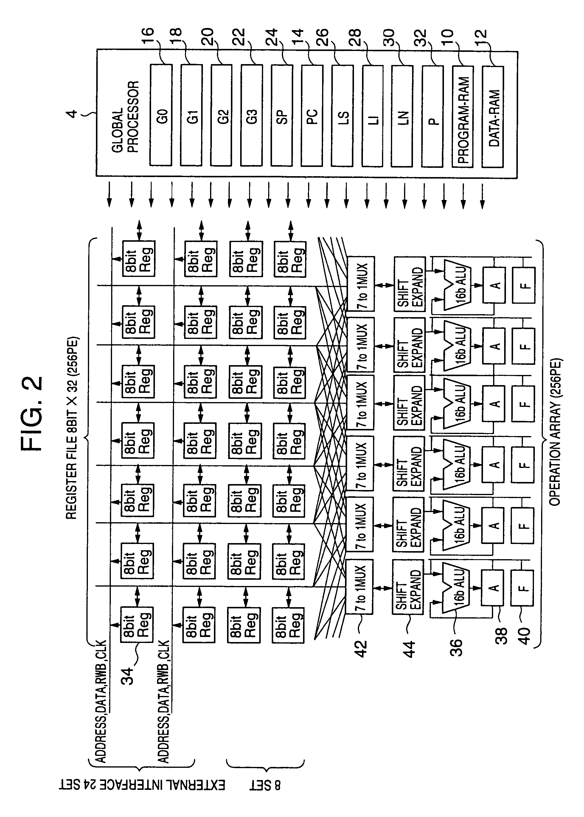
[0064]FIG. 3 shows a block diagram of an SIMD microprocessor according to the first embodiment of the present invention, especially shows enlarged one PE3 portion.

[0065]An operation array 8 of each PE includes:

[0066]an ALU 36;

[0067]two ALU latches (ALT[1]50-1, ALT[2]502);

[0068]an A register 38 for storing operation result;

[0069]two F registers utilized as temporary registers (F1 register 40-1, F2 register 40-2); and

[0070]a CF (carry flag) 54 for latching a carry output from the ALU 36.

[0071]A multiplexer 52 inserted between the A register 38 and the ALU 36, selects one data out of three data that are ALU 36 operation result, the contents of two ALU latches (ALT[1]50-1, ALT[2]50-2), and stores the selected data to the A register 38. Control signals for controlling selection by the multiplexer 52 are:

[0072]a control signal [1] from the global processor 4; and

[0073]the carry output from the ALU 36.

[0074]In the ALU 36, when executing normal operation instructions, the operation result o...

second embodiment

[0083]In case where two data to be compared are unsigned data, it is possible to judge the comparison result from the carry output. On the contrary, in case where the data to be compared are signed data, the comparison result should be judged from the EXCLUSIVE-OR of a negative bit (MSB of the subtraction result of the ALU 36) and an overflow bit.

[0084]FIG. 4 shows a block diagram of an SIMD type microprocessor 2 according to the second embodiment of the present invention, specifically shows an enlarged block diagram of one PE3 portion.

[0085]According to the structure shown in FIG. 4, both unsigned data and signed data can be processed. Each flag (C:carry, V:overflow, N:negative) outputted from the ALU 36 is inputted to a multiplexer 52 which selects the input to an A register 38, and to a flag register block (PSR) 68. In case where the comparison data are unsigned data, the multiplexer 52 selects data to be inputted to the A register 38, depending on the carry. In case where the co...


PUM


Abstract

An SIMD type microprocessor having a plurality of processor elements, wherein data stored in a specific register included in each processor element and data stored in an operand-designated source register are compared based on a first type of instruction; after the comparison, a larger data is stored in the specific register; and a smaller data is stored in the source register or an operand-designated destination register other than the source register.

Description

BACKGROUND OF THE INVENTION[0001]1. Field of the Invention[0002]The present invention relates to an SIMD (Single Instruction-stream Multiple Data-stream) type microprocessor.[0003]2. Description of the Related Art[0004]In SIMD microprocessors, one instruction can simultaneously perform the same operation processing on a plurality of data. Because of this performance, such microprocessors are frequently utilized in processing such as image processing in which the same operations are performed on a lot of data.[0005]In normal operation processing in an SIMD microprocessor, a plurality of operation units (Processor Elements (PE)) are arranged, and the same operations are simultaneously performed on a plurality of data. In this manner, high speed operation processing can be achieved.[0006]In “image data processing”, a variety of filtering processing ways are performed in order to correct image quality. Normal filtering processing uses a weighted operation of an object pixel and pixels a...

Claims


Application Information

Patent Timeline
IPC IPC(8): G06F7/22G06F9/38G06F7/08G06F7/24G06F7/544G06F9/30G06F9/305G06F15/80G06F17/10G06T1/20G06T5/20
CPCG06F7/24G06F7/544G06F9/30021G06F9/30025G06F2207/3828G06T5/20G06T2200/28G06F9/30036
Inventor IWANAGA, KAZUHIKO
Owner RICOH KK
Why Eureka
Try Eureka