
Semiconductor device having a channel extending vertically

a vertically extending, semiconductor technology, applied in the direction of semiconductor devices, electrical devices, transistors, etc., can solve the problems of slowing down the operation speed affecting the operation efficiency of the conventional transistor, so as to achieve the effect of reducing the operation failure of the semiconductor device due to relatively fast operation speed of the semiconductor device, and reducing the accumulation of holes in the body

Inactive Publication Date: 2009-02-10
SAMSUNG ELECTRONICS CO LTD
View PDF6 Cites 11 Cited by
  • Summary
  • Abstract
  • Description
  • Claims
  • Application Information

AI Technical Summary

Benefits of technology

[0022]According to the present invention, a semiconductor device includes a body that is not isolated by source / drain regions. In addition, a width of a channel generated in the semiconductor device is large so that an operation speed of the semiconductor device may be relatively fast. Because the source / drain regions may not isolate the body, an accumulation of holes in the body may be efficiently prevented. As a result, an operation failure of a semiconductor device due to the accumulation of the holes in the body may be reduced.

Problems solved by technology

Thus, operation characteristics of the conventional transistor may be degraded due to a floating body effect.
Thus, a current operation capability of the conventional transistor may be relatively poor and thus slow down operation speed of the conventional transistor.
In addition, processes for forming the body line and the word line on the first sidewall and the second sidewall, respectively, are relatively complicated.

Method used


Image

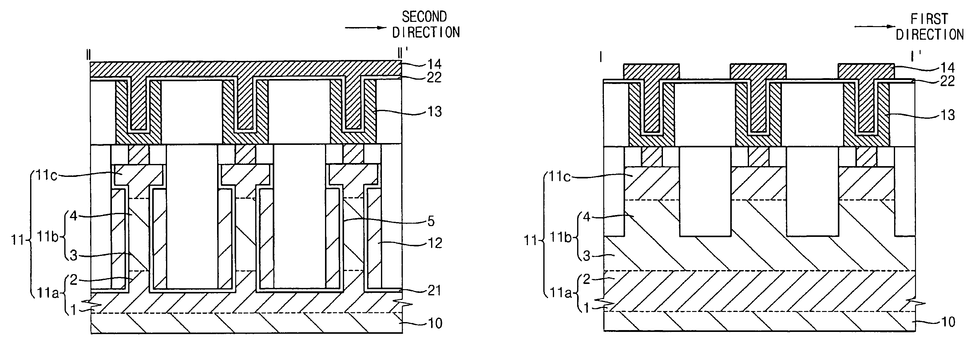
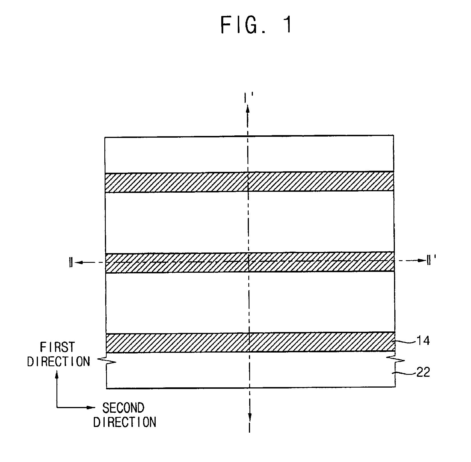
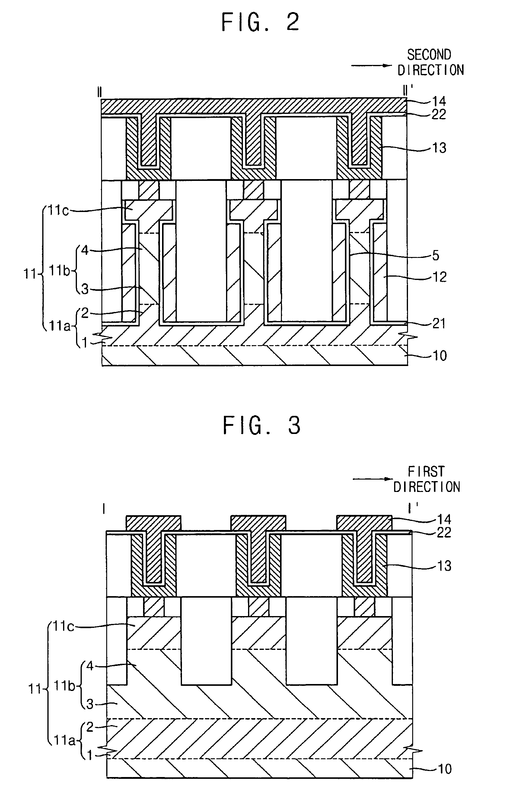
  • Semiconductor device having a channel extending vertically
  • Semiconductor device having a channel extending vertically
  • Semiconductor device having a channel extending vertically

Examples


Embodiment Construction

[0031]Embodiments of the present invention will be described with reference to the accompanying drawings. It will be understood that when an element or layer is referred to as being “on,”“connected to” and / or “coupled to” another element or layer, the element or layer may be directly on, connected and / or coupled to the other element or layer or intervening elements or layers may be present. In contrast, when an element is referred to as being “directly on,”“directly connected to” and / or “directly coupled to” another element or layer, no intervening elements or layers are present. As used herein, the term “and / or” may include any and all combinations of one or more of the associated listed items.

[0032]It will also be understood that, although the terms first, second, etc. may be used herein to describe various elements, components, regions, layers and / or sections. These elements, components, regions, layers and / or sections should not be limited by these terms. These terms may be used...


PUM


Abstract

In a semiconductor device, the semiconductor device includes a conductive structure, first insulating layers and first conductive layer patterns. The conductive structure includes a first portion, second portions and third portions. The second portions extend in a first direction on the first portion. The second portions are spaced apart from one another in a second direction substantially perpendicular to the first direction. The third portions are provided on the second portions. The third portions are spaced apart from one another in the first and second directions. The first insulating layers cover sidewalls of the second portions. The first conductive layer patterns are provided on the first insulating layers.

Description

CROSS-REFERENCE TO RELATED APPLICATION[0001]This application claims priority under 35 U.S.C. §119 to Korean Patent Application No. 10-2006-0008313 filed on Jan. 26, 2006, the contents of which are incorporated herein by reference in their entirety.BACKGROUND OF THE INVENTION[0002]1. Field of the Invention[0003]The present invention relates to a semiconductor device and a method of manufacturing the semiconductor device. More particularly, the present invention relates to a semiconductor device in which a channel extending vertically is generated, and a method of manufacturing the semiconductor device.[0004]2. Description of the Related Art[0005]A transistor includes a source region, a drain region, a body, an electrode and an insulating layer. The insulating layer electrically insulates the electrode from the source region, the drain region and the body. The electrode applies a voltage to the body.[0006]An example of a conventional transistor having a body extending vertically is di...

Claims


Application Information

Patent Timeline
Patent Type & Authority Patents(United States)
IPC IPC(8): H01L21/336
CPCH01L27/10823H01L27/10876H01L29/66666H01L29/7827H10B12/34H10B12/053H01L21/18
Inventor RHIE, HYOUNG-SEUB
Owner SAMSUNG ELECTRONICS CO LTD
Learn More