Microelectronic package optionally having differing cover and device thermal expansivities

a technology of microelectronic packages and covers, applied in the direction of electrical apparatus, semiconductor devices, semiconductor/solid-state device details, etc., can solve the problems of exacerbated cte mismatch between the cover and the wafer, and the typical close matching of the wafer-level manufacturing of microelectronic packages, so as to achieve substantial differences in thermal expansion coefficients and effective stiffness

Inactive Publication Date: 2009-02-03
TESSERA INC
View PDF8 Cites 17 Cited by
  • Summary
  • Abstract
  • Description
  • Claims
  • Application Information

AI Technical Summary

Problems solved by technology

As described in more detail below, problems associated with CTE mismatch between the wafer and the cover is exacerbated due to the size of the wafer-level assembly.
Thus, wafer-level manufacturing of microelectronic packages typically requires exceptionally close matching of device and substrate CTE.

Method used


Image

  • Microelectronic package optionally having differing cover and device thermal expansivities
  • Microelectronic package optionally having differing cover and device thermal expansivities
  • Microelectronic package optionally having differing cover and device thermal expansivities

Examples


Embodiment Construction

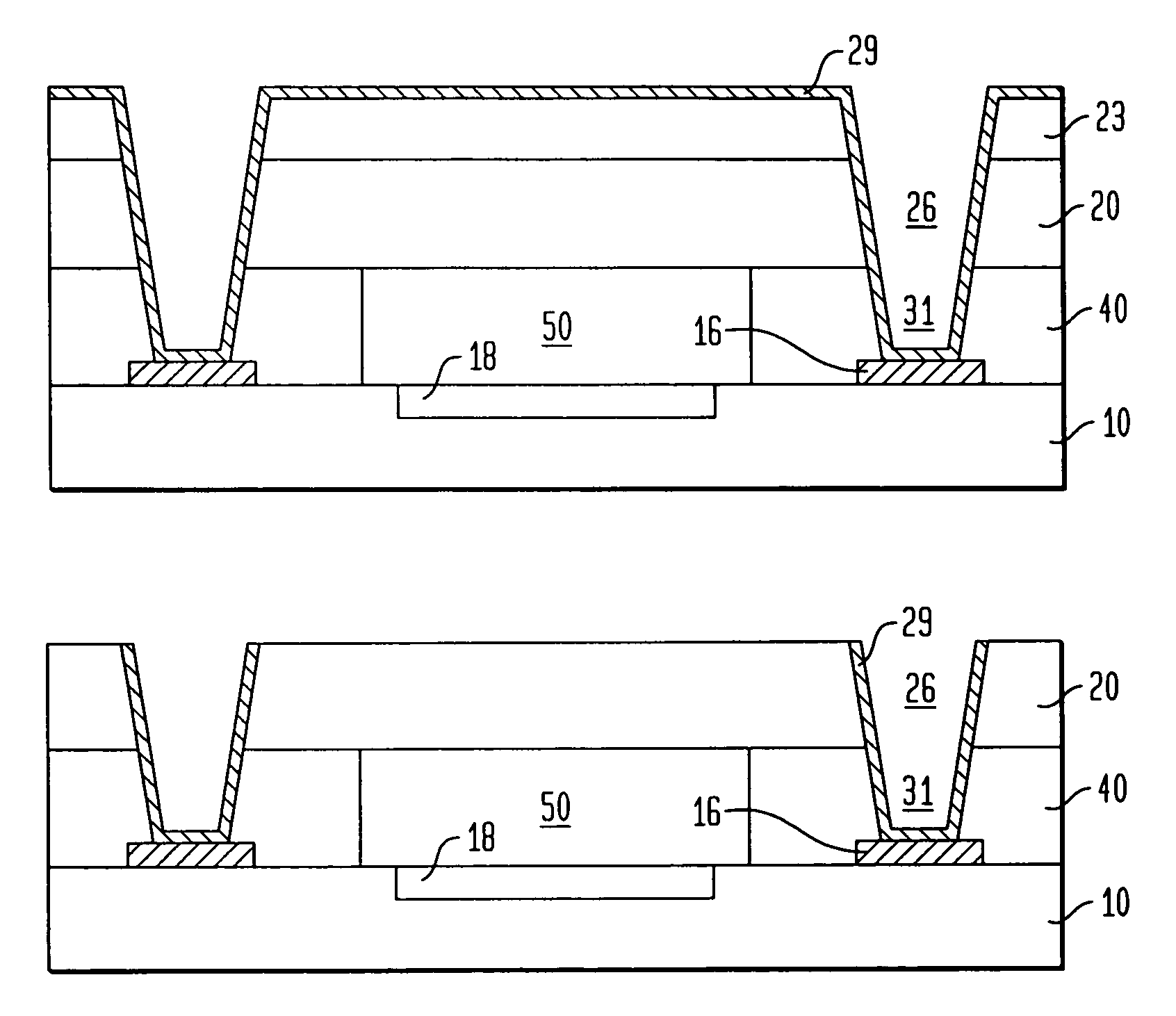
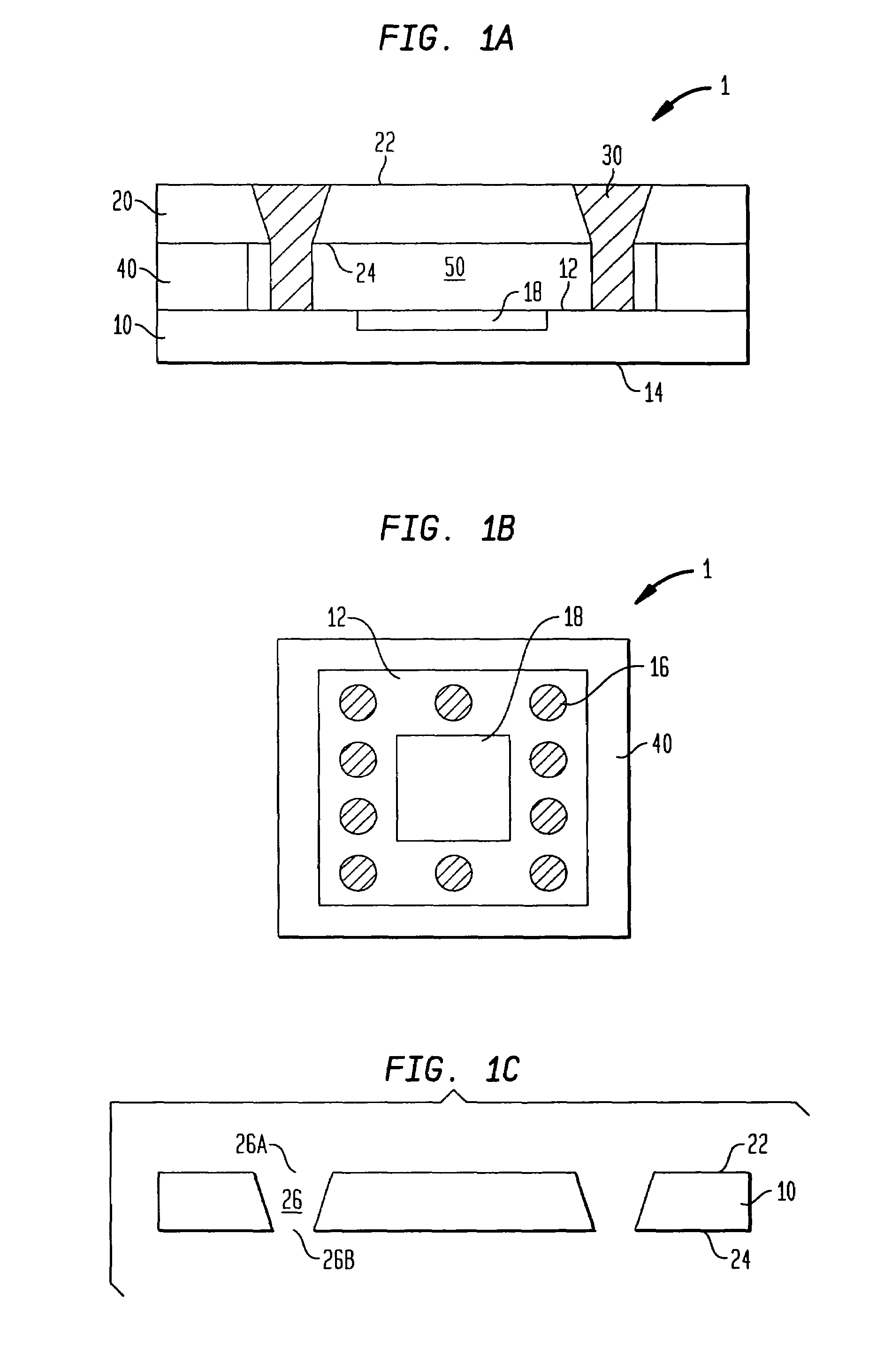
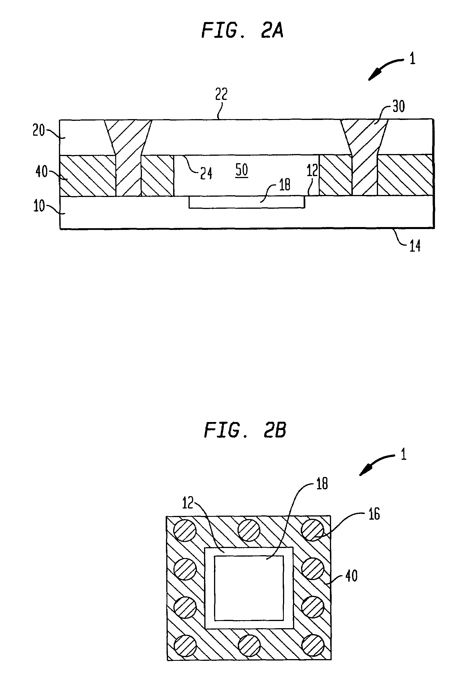
[0032]Before describing the present invention in detail, it is to be understood that the invention is not limited to specific microelectronic devices or types of electronic products, as such may vary. It is also to be understood that the terminology used herein is for the purpose of describing particular embodiments only, and is not intended to be limiting.

[0033]As used in this specification and the appended claims, the singular article forms “a,”“an,” and “the” include both singular and plural referents unless the context clearly dictates otherwise. Thus, for example, reference to “a cavity,” includes a plurality of cavities as well as a single conductive region, reference to “a microelectronic device” includes a single device as well as a combination of devices, and the like.

[0034]In addition, terminology indicative or suggestive of a particular spatial relationship between elements of the invention is to be construed in a relative sense rather an absolute sense unless the context...


PUM


Abstract

A microelectronic package is provided that includes a microelectronic device and a cover. The device and the cover are typically substantially immobilized relative to each other. The cover typically has a higher coefficient of thermal expansion while the device has a higher effective stiffness. The package may be formed in wafer-level processes.

Description

FIELD OF THE INVENTION[0001]The invention relates generally to microelectronic packages that include a microelectronic device and a cover and an optional cavity therebetween. In particular, the invention relates to packages that include devices and covers that may have differing thermal expansivities, differing effective stiffnesses, coatings and / or layers. Also provided are wafer-level microelectronic assemblies and methods for forming microelectronic packages and assemblies.BACKGROUND OF THE INVENTION[0002]Microelectronic devices such as semiconductor chips are flat bodies with contacts disposed on the front surface that are connected to the internal electrical circuitry of the chip itself. To facilitate ease in handling, testing and other processes associated with product manufacturing, semiconductor chips are typically provided in microelectronic packages having terminals that are electrically connected to the chip contacts. The package may then be connected to test equipment to...

Claims


Application Information

Patent Timeline
Patent Type & Authority Patents(United States)
IPC IPC(8): H01L23/12
CPCH01L23/06H01L2924/01079H01L2924/12044H01L2924/0002H01L2924/00
Inventor TUCKERMAN, DAVID B.HUMPSTON, GILES
Owner TESSERA INC
Why Eureka
Try Eureka