
Semiconductor device and fabrication process thereof

a technology of semiconductor devices and fabrication processes, applied in semiconductor devices, semiconductor/solid-state device details, electrical devices, etc., can solve the problems of poor strength, poor inability to qualify for resin sealing techniques in prior art techniques, so as to improve strength and reliability of resin sealing, prevent fabrication problems, and improve performance and quality

Active Publication Date: 2008-12-16
SHENZHEN TOREY MICROELECTRONIC TECH CO LTD
View PDF16 Cites 2 Cited by
  • Summary
  • Abstract
  • Description
  • Claims
  • Application Information

AI Technical Summary

Benefits of technology

[0017]The present invention was made in view of the foregoing problems, and it is an object of the present invention to provide a semiconductor device that excels in performance and quality, by improving strength and reliability of resin sealing and by preventing fabrication problems caused by “rise” of the insulating resin, and to provide a fabrication process of such a semiconductor device.
[0019]With this configuration, because the insulating resin contains a resin anti-repellent, a portion of the interconnection pattern around the semiconductor element can be prevented from being exposed in an area surrounded by the solder resist, when making electrical connections between the semiconductor element and the interconnection pattern. In addition, the resin fillet, which is formed under and around the semiconductor element, can increase in size. That is, the semiconductor element can be more firmly anchored on the insulating substrate.
[0020]As a result, the strength and reliability of resin sealing can be improved. Further, in the fabrication process, it is possible to prevent the problem of resin adhesion, which is caused when the insulating resin rises along the side surfaces of the semiconductor element and adheres to the pressure applying tool and / or heat applying tool used to apply pressure and / or heat to the semiconductor element, in connecting the semiconductor element with the interconnection pattern by applying pressure on the semiconductor element. These and other fabrication problems can thus be prevented.
[0022]With this fabrication process, because the insulating resin applied in the insulating resin applying step contains a resin anti-repellent, a portion of the interconnection pattern around the semiconductor element can be prevented from being exposed in an area surrounded by the solder resist, when making electrical connections between the semiconductor element and the interconnection pattern in the semiconductor element pressing step. In addition, the resin fillet, which is formed under and around the semiconductor element, can increase in size. That is, the semiconductor element can be more firmly anchored on the insulating substrate.
[0023]As a result, the strength and reliability of resin sealing can be improved. Further, in the fabrication process, it is possible to prevent the problem of resin adhesion, which is caused when the insulating resin rises along the side surfaces of the semiconductor element and adheres to the pressure applying tool and / or heat applying tool used to apply pressure and / or heat to the semiconductor element, in connecting the semiconductor element with the interconnection pattern by applying pressure on the semiconductor element. These and other fabrication problems can thus be prevented.

Problems solved by technology

One drawback of the foregoing conventional techniques is the poor strength and poor reliability of resin sealing.
Further, the foregoing publications are associated with fabrication problems caused by the insulating resin, when the insulating resin rises to the pressure applying tool or heat applying tool used to apply pressure or heat to the semiconductor element.
Therefore, the foregoing prior art techniques do not qualify as a technique for resin sealing.
This may lead to a problem that a portion of the interconnection pattern 2 around the semiconductor element 3 is exposed in an area surrounded by the solder resist 5.
Another deficiency is that the resin fillet, which is formed along the side surfaces of the semiconductor element to anchor the semiconductor element 3, cannot have enough size, with the result that the strength and reliability of resin sealing become poor.
This is problematic because the insulating resin 14 adheres to the pressure applying tool and / or heat applying tool used to apply pressure and / or heat to the semiconductor element 3.
The problem of “resin rise” as indicated by arrow F is even more problematic these days in light of the development of thinner semiconductor devices with a proportionally reduced thickness of the semiconductor elements.

Method used


Image

  • Semiconductor device and fabrication process thereof
  • Semiconductor device and fabrication process thereof
  • Semiconductor device and fabrication process thereof

Examples


first embodiment

[0029]One embodiment of the present invention is described below with reference to FIG. 1(a) through FIG. 1(e). It should be noted that the present invention is not limited by the following descriptions.

[0030]A semiconductor device of the present invention includes an interconnection pattern formed on an insulating substrate. A semiconductor element is electrically connected to the interconnection pattern via projecting electrodes. A resin layer and a resin fillet are formed around the semiconductor element and between the semiconductor element and the insulating substrate. In the semiconductor device of the present invention according to this configuration, the resin fillet is formed using an insulating resin containing a resin anti-repellent for adjusting wettability of the insulating resin.

[0031]More specifically, as shown in FIG. 1(e), the semiconductor device of the present embodiment includes a circuit board 20, a semiconductor element 3, and a resin fillet 11, among other com...

second embodiment

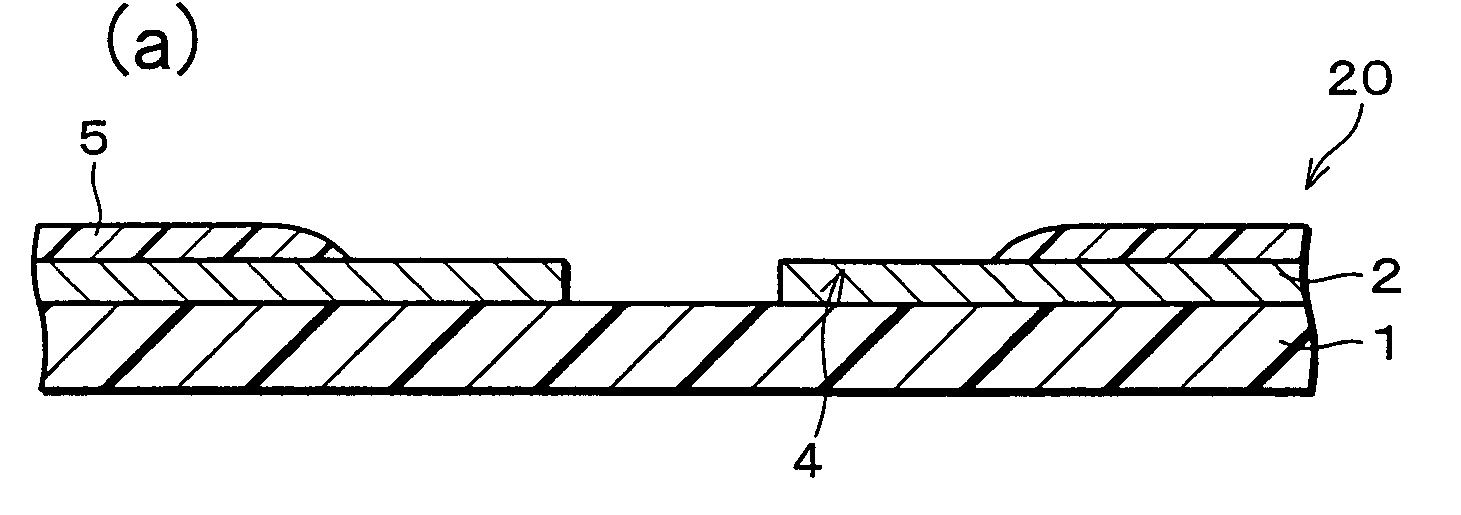
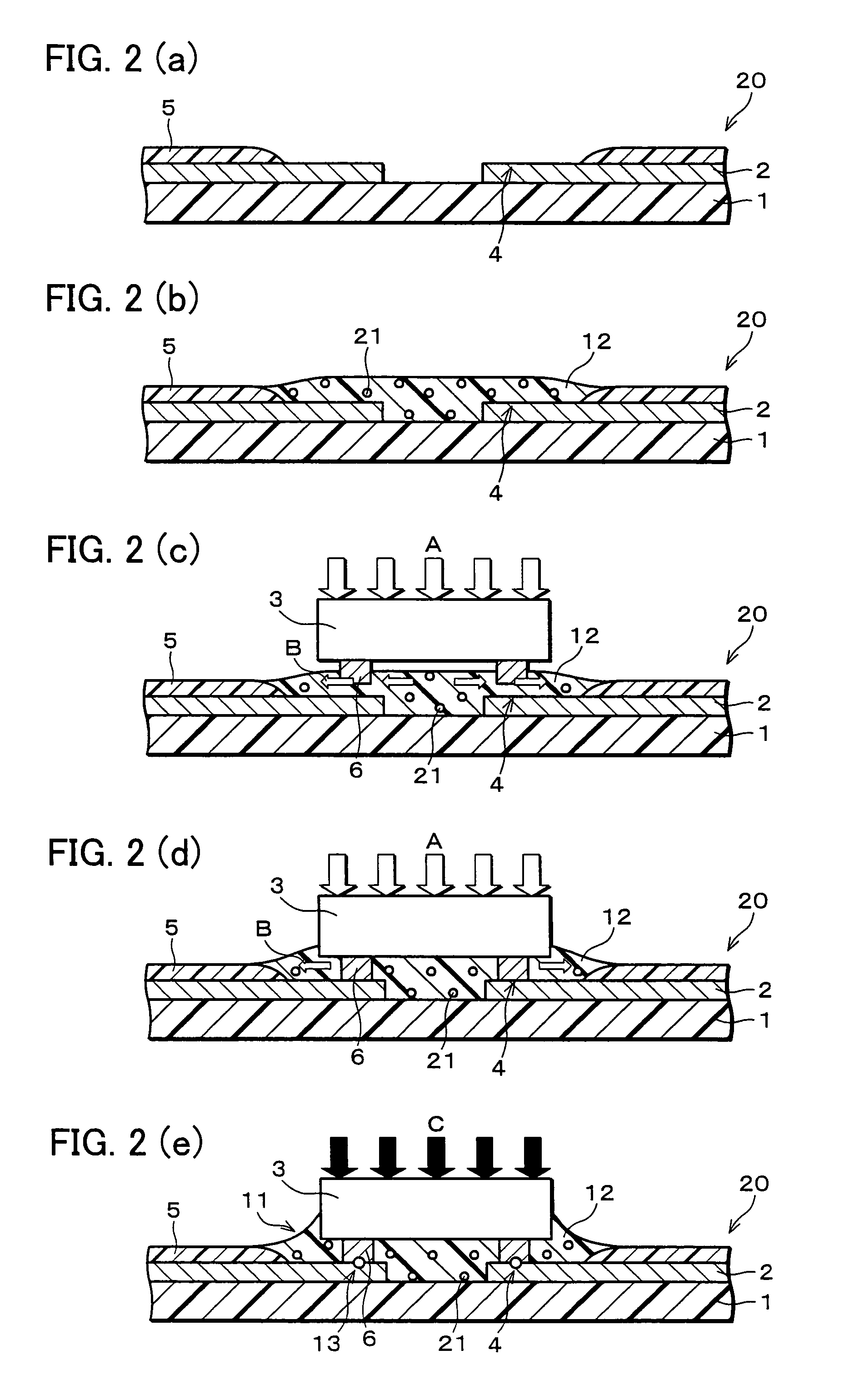
[0074]The following describes another embodiment of the present invention with reference to FIG. 2(a) through FIG. 2(e). It should be appreciated that the present invention is not limited by the following descriptions. For simplicity, elements having the same functions as those already described in the First Embodiment are given the same reference numerals and explanations thereof are omitted here.

[0075]In the First Embodiment, the resin fillet 11 is produced from the insulating resin 7 containing a resin anti-repellent. In the Second Embodiment, however, the resin fillet 11 is produced from an insulating resin 12 containing conductive particles 21 dispersed in the insulating resin 12, in addition to a resin anti-repellent, as shown in FIG. 2(e).

[0076]By the conductive particles 21 dispersed in the insulating resin 12 forming the resin fillet 11, the projecting electrodes 6 of the semiconductor element 3 and the contacts 4 of the interconnection pattern 2 on the insulating tape 1 ca...


PUM


Abstract

The semiconductor device uses an insulating resin that contains at least a resin anti-repellent for adjusting wettability of the insulating resin. The insulating resin is applied on a circuit board, and a semiconductor element is placed thereon and pressed against it. The applied pressure pushes out a portion of the insulating resin under the semiconductor element. This portion of the insulating resin combines with a portion of the insulating resin around the semiconductor element to form a resin fillet on the side surfaces of the semiconductor element.

Description

FIELD OF THE INVENTION[0001]The present invention relates to semiconductor devices and fabrication processes thereof, and particularly to COF (Chip on Film) semiconductor devices (“COF” hereinafter) in which a semiconductor element is bonded to a flexile circuit board, and to fabrication processes of such semiconductor devices.BACKGROUND OF THE INVENTION[0002]There has been rapid advancement in the field of electronic devices such as portable phones and portable information terminals in realizing smaller, thinner, and more lightweight devices. This progress has called for improvements in various components of these electronic devices, including a semiconductor device mounted in an electronic device, in terms of size, weight, function, performance, and packing density.[0003]Currently, in some semiconductor devices, one approach to realize higher packing density and to reduce thickness and weight of the device is to mount a semiconductor element on a circuit board that is realized by ...

Claims


Application Information

Patent Timeline
IPC IPC(8): H01L23/48H01L23/29H01L21/56H01L21/60H01L23/498
CPCH01L21/563H01L23/49816H01L24/29H01L23/49894H01L24/81H01L24/83H01L2224/26175H01L2224/83851H01L2224/293H01L2224/2929H01L2224/32225H01L2924/0665H01L2924/014H01L2924/01006H01L2224/2919H01L2924/14H01L2924/0781H01L2924/01082H01L2924/01079H01L2924/01078H01L2924/0105H01L23/4985H01L2224/16225H01L2224/73203H01L2224/73204H01L2224/81801H01L2224/83192H01L2224/838H01L2924/01004H01L2924/01005H01L2924/01029H01L2924/01033H01L2924/00H01L2924/00012H01L2924/00014H01L2224/0401H01L23/29
Inventor SEKO, TOSHIHARU
Owner SHENZHEN TOREY MICROELECTRONIC TECH CO LTD
Learn More