Semiconductor device and its manufacturing method, and display device and electronic appliance

a technology of semiconductor devices and manufacturing methods, applied in semiconductor devices, electrical appliances, instruments, etc., can solve the problems of light-emitting elements having lower luminous efficiency, and achieve the effects of improving the luminous efficiency of the display device, increasing the number of light exiting from the top surface per unit area, and prolonging the life of the display devi

Inactive Publication Date: 2008-10-21
SEMICON ENERGY LAB CO LTD
View PDF9 Cites 26 Cited by
  • Summary
  • Abstract
  • Description
  • Claims
  • Application Information

AI Technical Summary

Benefits of technology

[0010]In this semiconductor device, the first electrode, the semiconductor layer of the first conductivity type, the light-emitting layer, and the semiconductor layer of the second conductivity type are formed along the bottom surface and the side surface of the first depressed portion or opening portion formed in the insulating film. Thus, light emitted from the light-emitting layer exits from a top surface of a light-emitting element after passing through the semiconductor layer of the second conductivity type. Therefore, the light emitted from the light-emitting layer exits from the top surface of the light-emitting element efficiently.
[0011]When the semiconductor layer of the second conductivity type has a smaller band gap than the light-emitting layer, the semiconductor layer of the second conductivity type is preferably thinner than the light-emitting layer. This makes it possible to suppress the absorption of light emitted from the light-emitting layer in the semiconductor layer of the second conductivity type.
[0013]In this semiconductor device, since the end face of the light-emitting layer has an angle of more than 90° and less than 270° to the surface of the insulating film, light emitted from the light-emitting layer exits upward from the end face of the light-emitting layer. Therefore, the light emitted from the light-emitting layer exits from the top surface of the light-emitting element efficiently.
[0016]The first electrode preferably has a reflectance of 90% or more with respect to light emitted from the light-emitting layer. In this case, light emitted downward from the light-emitting layer is reflected off the first electrode and exits from the top surface of the light-emitting element. Therefore, the light emitted from the light-emitting layer exits from the top surface of the light-emitting element further efficiently.
[0028]In accordance with the present invention, as described above, light emitted from the light-emitting layer can exit from the top surface of the light-emitting element efficiently. Moreover, the intensity of light which exits from the top surface per unit area can be increased. In addition, a display device can be formed in which ultraviolet light emitted from the light-emitting element is absorbed by a fluorescent film or the like and this fluorescent film emits R, G or B light. Therefore, the luminous efficiency of the display device can be improved. Furthermore, the lifetime of the display device can be made longer than that of a display device using organic EL.

Problems solved by technology

However, since the transparent electrode has high resistance, the transparent electrode consumes electric power to cause the light-emitting element to have lower luminous efficiency.

Method used


Image

  • Semiconductor device and its manufacturing method, and display device and electronic appliance
  • Semiconductor device and its manufacturing method, and display device and electronic appliance
  • Semiconductor device and its manufacturing method, and display device and electronic appliance

Examples


embodiment mode 1

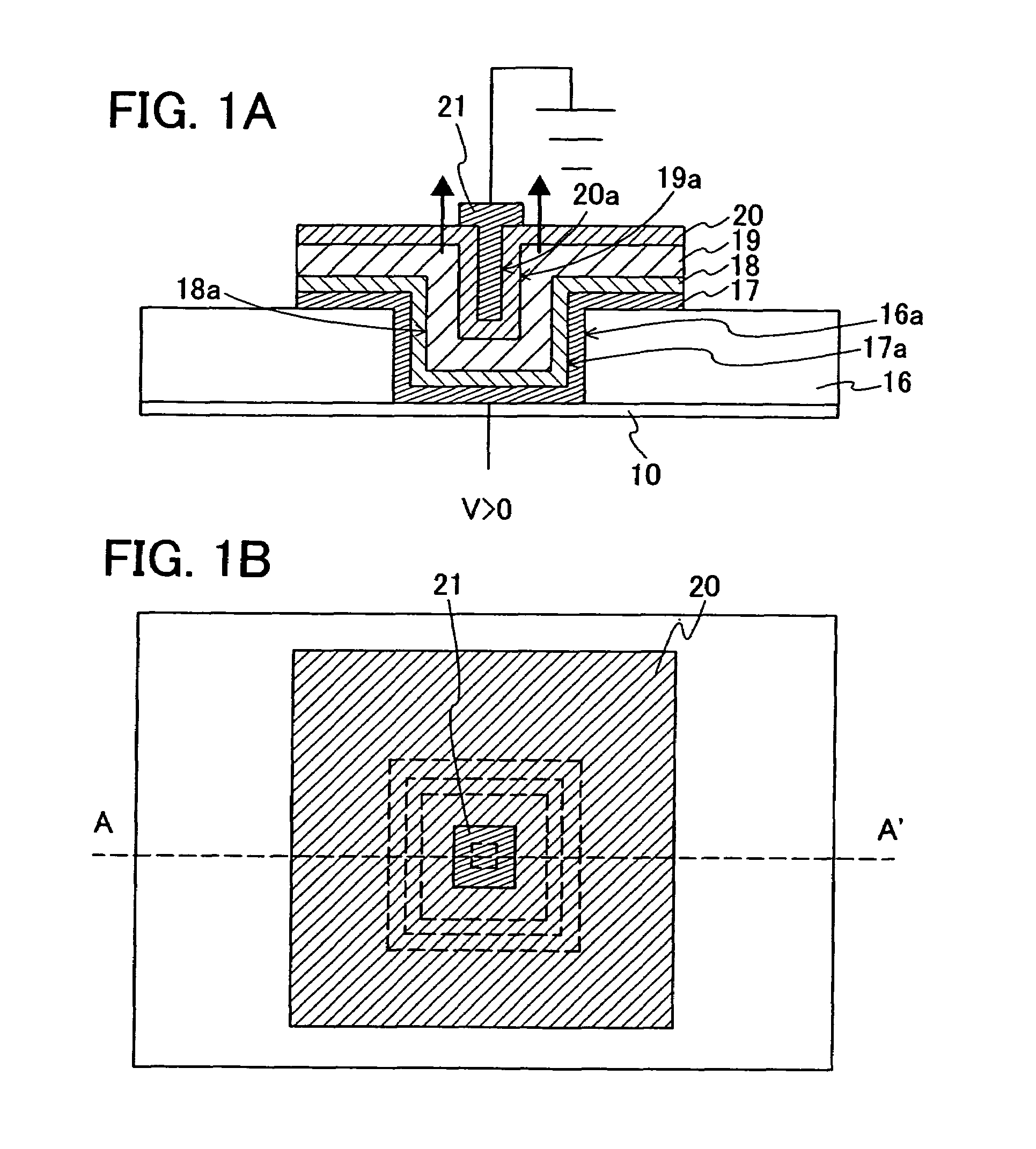
[0046]An embodiment mode of the present invention will hereinafter be described with reference to drawings. FIG. 1A is a cross-sectional view for explaining a structure of a light-emitting element in accordance with Embodiment Mode 1 of the present invention. FIG. 1B is a plan view of this light-emitting element. It is to be noted that FIG. 1A shows a cross section along a line A-A′ of FIG. 1B. In this light-emitting element, an insulating film 16 is formed over a substrate 10. The substrate 10 is, for example, a glass substrate. The insulating film 16 is, for example, a silicon oxide film with a thickness of, for example, 0.5 to 1.5 μm. An opening portion 16a is formed in the insulating film 16. A bottom surface of the opening portion 16a is, for example, a square with a length of 2.5 μm on a side.

[0047]A lower electrode 17 is formed over the insulating film 16 around the opening portion 16a and over a bottom surface and a side surface of the opening portion 16a. The lower electrod...

embodiment mode 2

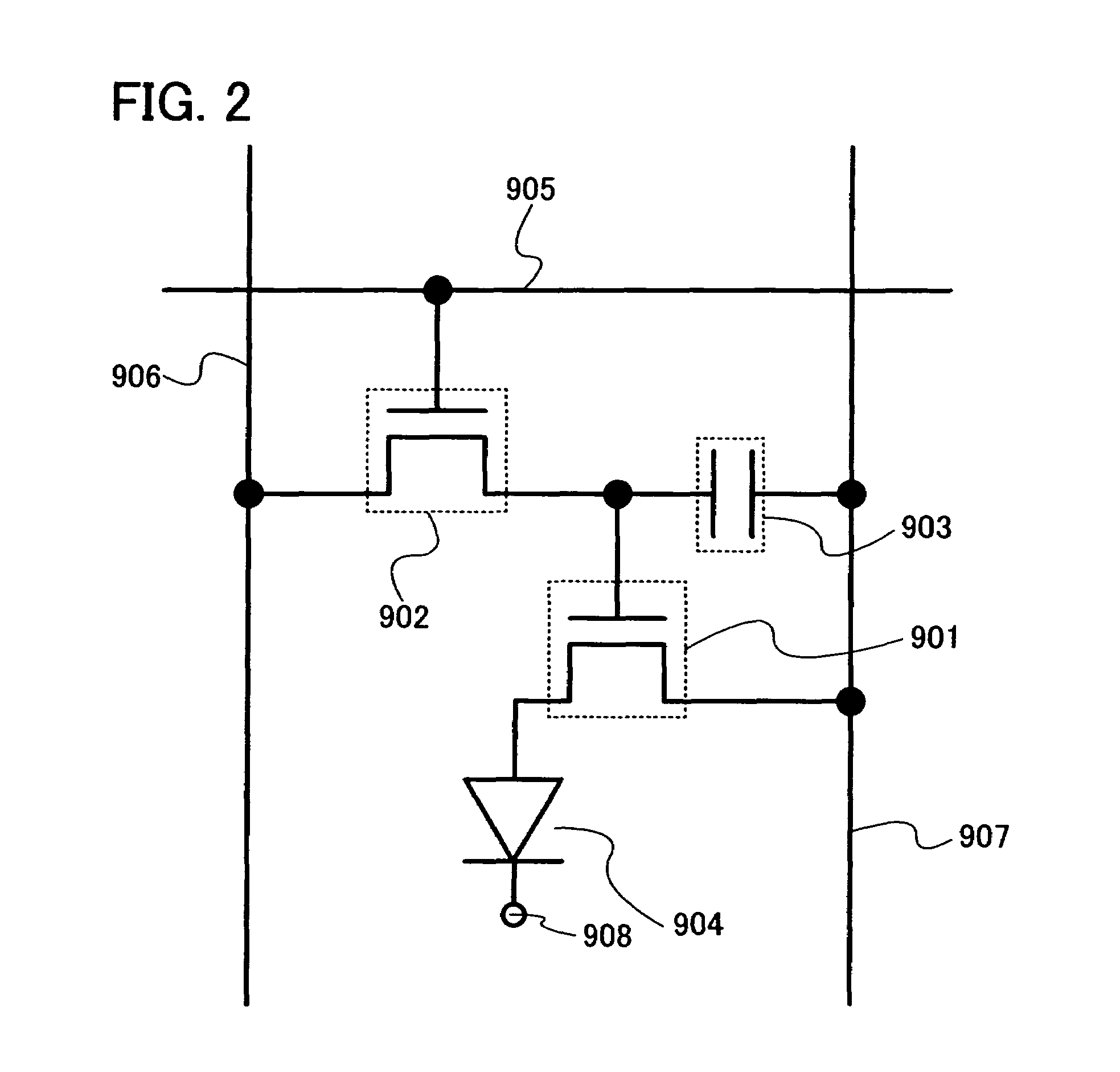
[0066]FIG. 2 is a circuit diagram for explaining a structure of a driving circuit of a light-emitting element in accordance with Embodiment Mode 2 of the present invention. In this embodiment mode, a light-emitting element 904 has a similar structure to that of the light-emitting element described in Embodiment Mode 1, and a counter electrode 908 corresponds to the upper electrode 21 of FIGS. 1A and 1B. An electrode corresponding to the lower electrode 17 is electrically connected to a power source line 907 with a driving TFT (thin film transistor) 901 interposed therebetween. A gate electrode of the driving TFT 901 is electrically connected to a signal line 906 with a switching TFT 902 interposed therebetween. A gate electrode of the switching TFT 902 is electrically connected to a scan line 905. It is to be noted that the gate electrode of the driving TFT 901 is also connected to the power source line 907 with a capacitor element 903 interposed therebetween.

[0067]In such a circuit...

embodiment mode 3

[0069]FIG. 3A is a cross-sectional view and FIG. 3B is a plan view, both explaining a structure of a light-emitting element in accordance with Embodiment Mode 3. It is to be noted that FIG. 3A shows a cross section along a line A-A′ of FIG. 3B. The light-emitting element shown in this embodiment mode has the same structure as the light-emitting element shown in FIGS. 1A and 1B except that a portion protruding upward from the surface of the insulating film 16 is removed. Therefore, the content described in Embodiment Mode 1 can also be applied to this embodiment mode except that emitted light exits directly from an end face of the light-emitting layer 19. A structure similar to that of Embodiment Mode 1 is denoted by the same reference numeral and the description thereof is omitted hereinafter.

[0070]A manufacturing method of the light-emitting element of this embodiment mode is as follows. First, the insulating film 16 and the opening portion 16a are formed over the substrate 10. Mor...


PUM


Abstract

A semiconductor device having a light-emitting element with excellent light-emitting characteristics is provided. The semiconductor device is provided with a first depressed portion or opening portion formed in an insulating film; a first electrode which is formed over the insulating film around the first depressed portion or opening portion, which is positioned in the first depressed portion or opening portion, and which forms a second depressed portion together with the first depressed portion or opening portion; a semiconductor layer of a first conductivity type which is formed over the first electrode and which forms a third depressed portion together with the second depressed portion; a light-emitting layer which is formed over the semiconductor layer of the first conductivity type and which forms a fourth depressed portion together with the third depressed portion; a semiconductor layer of a second conductivity type which is formed over the light-emitting layer and which forms a fifth depressed portion together with the fourth depressed portion; and a second electrode formed over the semiconductor layer of the second conductivity type that forms a bottom surface and a side surface of the fifth depressed portion.

Description

BACKGROUND OF THE INVENTION[0001]1. Field of the Invention[0002]The present invention relates to a semiconductor device, a display device, and an electronic appliance each having a light-emitting element with excellent light-emitting characteristics and also relates to a manufacturing method of a semiconductor device.[0003]2. Description of the Related Art[0004]FIG. 16 is a drawing for explaining a structure of a conventional light-emitting element. The conventional light-emitting element has a structure in which a lower electrode 1002, a semiconductor layer 1004 of a first conductivity type, a light-emitting layer 1006, a semiconductor layer 1008 of a second conductivity type, and an upper electrode 1010 are stacked over an insulating film 1000 in this order. When a predetermined potential is given to each of the lower electrode 1002 and the upper electrode 1010, excitons are recombined in the light-emitting layer 1006 and the energy released at the recombination is emitted as ligh...

Claims


Application Information

Patent Timeline
Patent Type & Authority Patents(United States)
IPC IPC(8): H01L29/04H01L33/24
CPCH01L33/24H01L29/7869H01L33/285
Inventor HONDA, TATSUYA
Owner SEMICON ENERGY LAB CO LTD
Why Eureka
Try Eureka