CMOS image sensor with reduced 1/f noise

a cmos image sensor and pixel circuit technology, applied in the field of cmos image sensors, can solve the problems of inability to increase the size of the source follower transistor, inability to modify the cmos process, and inability to achieve the effect of reducing the noise of the pixel circui

Active Publication Date: 2008-10-07
APTINA IMAGING CORP
View PDF3 Cites 3 Cited by
  • Summary
  • Abstract
  • Description
  • Claims
  • Application Information

AI Technical Summary

Benefits of technology

[0005]One form of the present invention provides a CMOS image sensor that includes a plurality of pixel circuits. Each pixel circuit includes a plurality of transistors. The image sensor includes a controller for controlling operation of the plurality of pixel circuits, wherein the controller is configured to cause at least one of the transistors in each pixel circuit to be placed in an accumulation mode and then switched from the accumulation mode to a strong inversion mode, thereby reducing 1 / f noise of the pixel circuits.

Problems solved by technology

Rather, in 3T pixel implementations, the read noise is typically dominated by “kTC” noise, which is the noise associated with resetting the pixel to a reset level.
Nonetheless, 1 / f noise from the source follower transistor provides a significant contribution to the overall noise in 3T pixel implementations.
However, due to pixel size constraints in CMOS image sensors, the size of the source follower transistor cannot typically be increased.
And modification of the CMOS process is typically complex and not a viable option.

Method used


Image

  • CMOS image sensor with reduced 1/f noise
  • CMOS image sensor with reduced 1/f noise
  • CMOS image sensor with reduced 1/f noise

Examples


Embodiment Construction

[0012]In the following detailed description of the preferred embodiments, reference is made to the accompanying drawings, which form a part hereof, and in which is shown by way of illustration specific embodiments in which the invention may be practiced. It is to be understood that other embodiments may be utilized and structural or logical changes may be made without departing from the scope of the present invention. The following detailed description, therefore, is not to be taken in a limiting sense, and the scope of the present invention is defined by the appended claims.

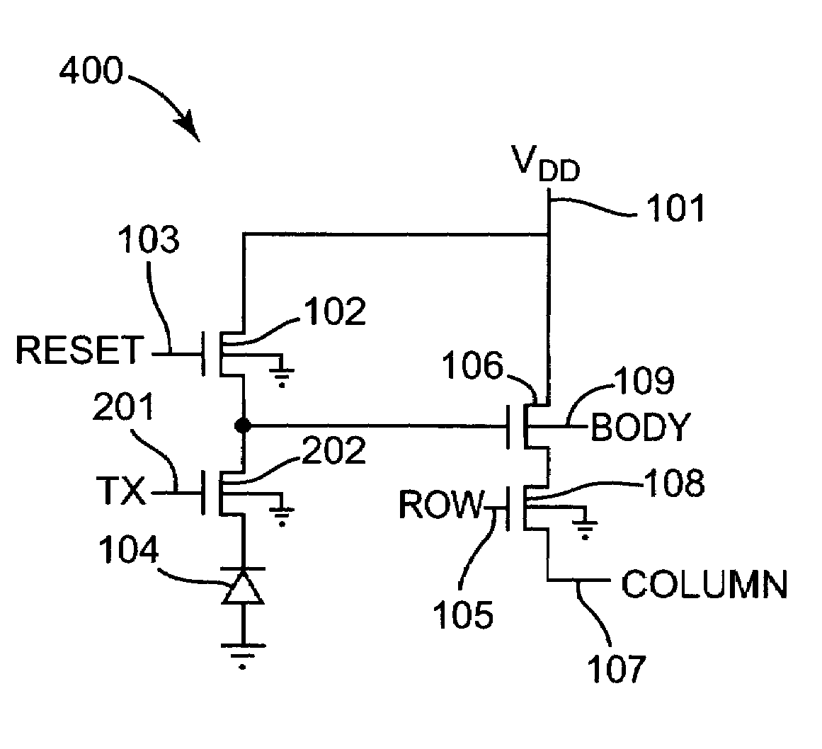
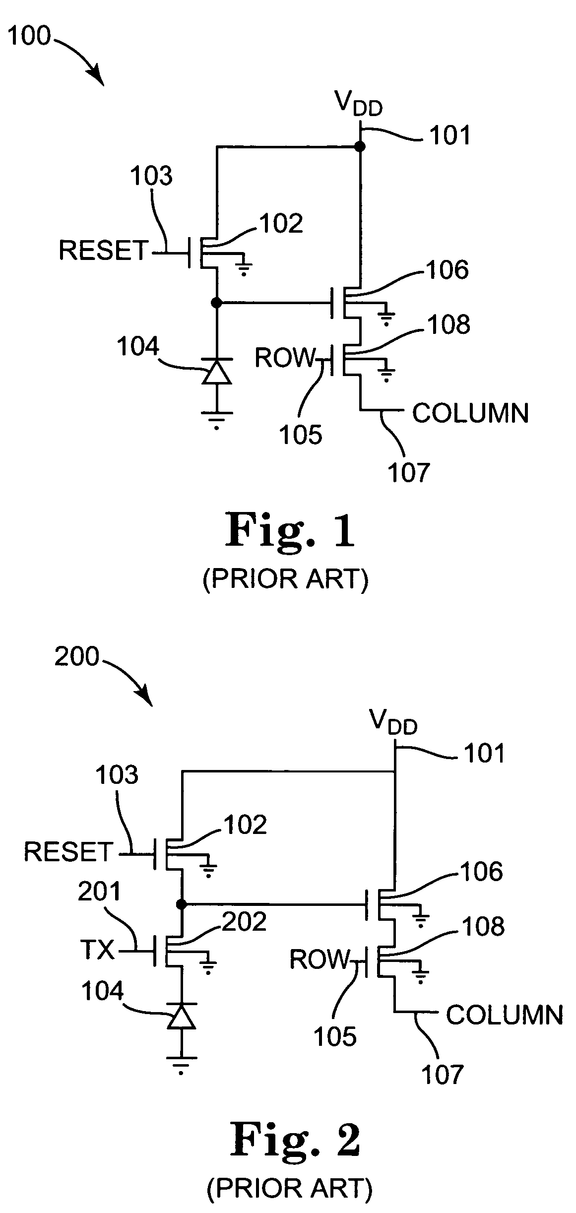
[0013]FIG. 1 is a schematic diagram illustrating a prior art three-transistor (3T) pixel circuit 100 for a CMOS image sensor. Pixel circuit 100 includes transistors 102, 106, and 108, and photodiode 104. Transistors 102, 106, and 108 are typically NMOS field effect transistors (FETs). The drain of transistor 102 is connected to voltage supply line 101 (VDD). The gate of transistor 102 is connected to a RESET lin...


PUM


Abstract

A CMOS image sensor includes a plurality of pixel circuits. Each pixel circuit includes a plurality of transistors. The image sensor includes a controller for controlling operation of the plurality of pixel circuits, wherein the controller is configured to cause at least one of the transistors in each pixel circuit to be placed in an accumulation mode and then switched from the accumulation mode to a strong inversion mode, thereby reducing 1 / f noise of the pixel circuits.

Description

THE FIELD OF THE INVENTION[0001]This invention relates generally to CMOS image sensors, and relates more particularly to a CMOS image sensor with reduced 1 / f noise.BACKGROUND OF THE INVENTION[0002]One type of prior art image sensor is an active pixel sensor (APS) image sensor. APS image sensors are typically fabricated using Complimentary Metal Oxide Semiconductor (CMOS) processing technology, and are also typically referred to as CMOS image sensors. CMOS image sensors sense light by converting incident light (photons) into electronic charge (electrons) via the photoelectric effect. Color CMOS image sensors are typically made by coating each individual pixel with a filter color (e.g. red, green, and blue). CMOS image sensors typically include a photo sensor (e.g., photodiode) and several CMOS transistors for each pixel. Some CMOS image sensors provide integrated analog-to-digital conversion and full timing control on a single integrated circuit.[0003]Existing CMOS image sensors incl...

Claims


Application Information

Patent Timeline
Patent Type & Authority Patents(United States)
IPC IPC(8): H04N3/14H04N5/217H04N5/335H01L27/146H01L31/10H04N5/357H04N5/374
CPCH04N5/357H04N5/374H04N25/60H04N25/76H04N3/1568
Inventor FOWLER, BOYD A. S.
Owner APTINA IMAGING CORP
Why Eureka
Try Eureka