Test and debug processor and method

a processor and debugging technology, applied in the field of electronic devices, can solve the problems of increasing the difficulty of debugging circuit boards after being assembled, needing synchronization, and wasting substantial time, and achieve the effect of increasing test speed and adding a lot of speed

Inactive Publication Date: 2008-09-23
MICHAEL SAM
View PDF21 Cites 7 Cited by
  • Summary
  • Abstract
  • Description
  • Claims
  • Application Information

AI Technical Summary

Benefits of technology

[0016]It is an object of the present invention to provide a test and debug processor that can execute test instructions without the involvement of the main CPU.
[0021]The test and debug processor is designed to directly access any memory location. This spares the test application a lot of time since the main CPU does not have to keep shuffling data back and forth from the memory. So in a normal case where the main CPU has to calculate the address of the test object to be sent out, read it in to a register inside the CPU, read the address of the test-bus controller, and then write the data to the controller, the controller can directly read the data from memory in a single cycle and send it out via the test bus. The same process will occur when the test processor reads the data back from the test board and stores it in memory. So integrating the memory access logic into the test-bus controller saves a lot of time normally needed to access the data objects.
[0023]Any of these features if integrated in the current solution will help increase the test speed. Combining all of these features in a single solution adds a lot of speed to the existing solution.

Problems solved by technology

With the complexity and increase of pin-count of new computer chips and the dense assembly of these chips on circuit boards, it becomes increasingly difficult to test and debug the circuit boards after being assembled.
It should be understood that a substantial amount of time is wasted due to the relatively extensive communications between the test-tool CPU, the memory and the test-bus controller.
One of the major difficulties of adding an instruction FIFO is the need to synchronize the instruction FIFO with the data FIFO.
Secondly, because the test-bus controller cannot execute any logic operations, it has to wait for the main CPU to execute these operations to test the incoming data from the test board.
With the current solution, it is difficult to add an Arithmetic-Logic Unit (hereinafter known as ALU) since the data is read and written in a FIFO, which cannot be addressed reliably since the data location in the FIFO depends on the speed of the main CPU and the speed of the test-bus connected to the test board.
Thirdly, because the test-bus controller cannot directly address and access the memory where the test data is stored, the main CPU (or a DMA channel) must act as the bridge between the test-bus controller and the memory where the test data is stored.
This task is very time consuming.

Method used


Image

  • Test and debug processor and method
  • Test and debug processor and method
  • Test and debug processor and method

Examples


Embodiment Construction

)

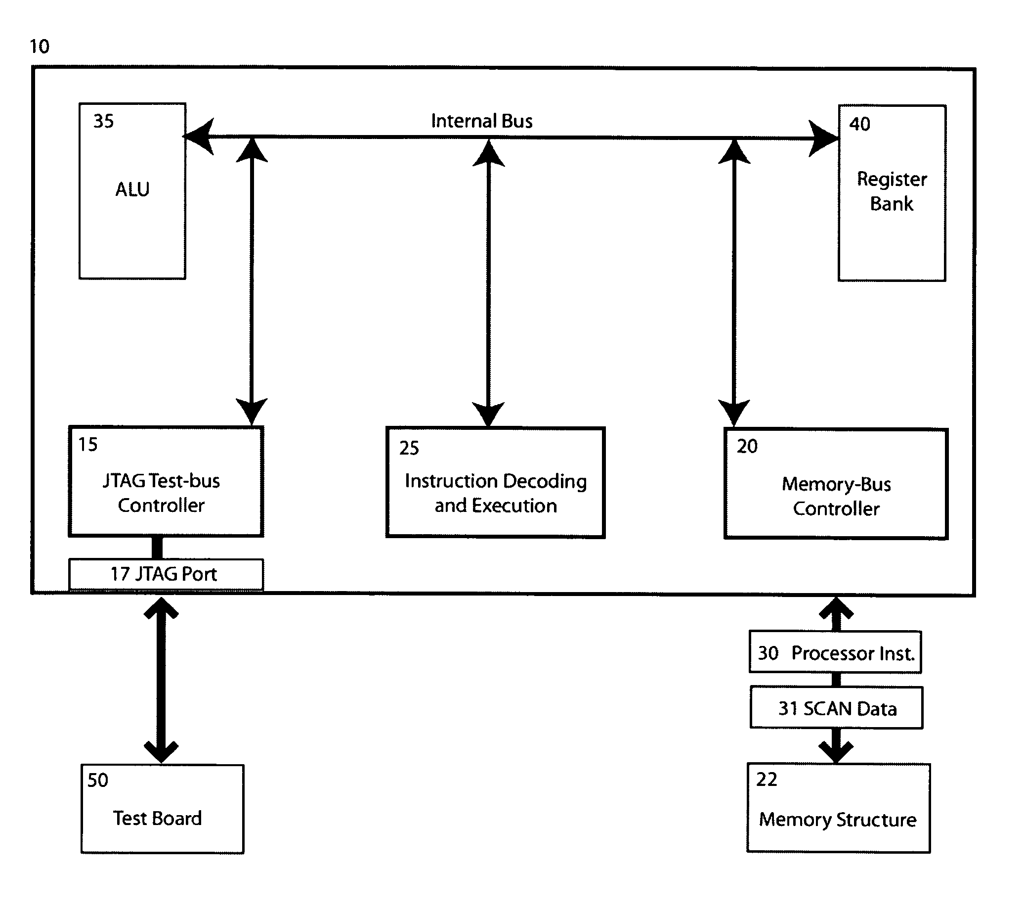
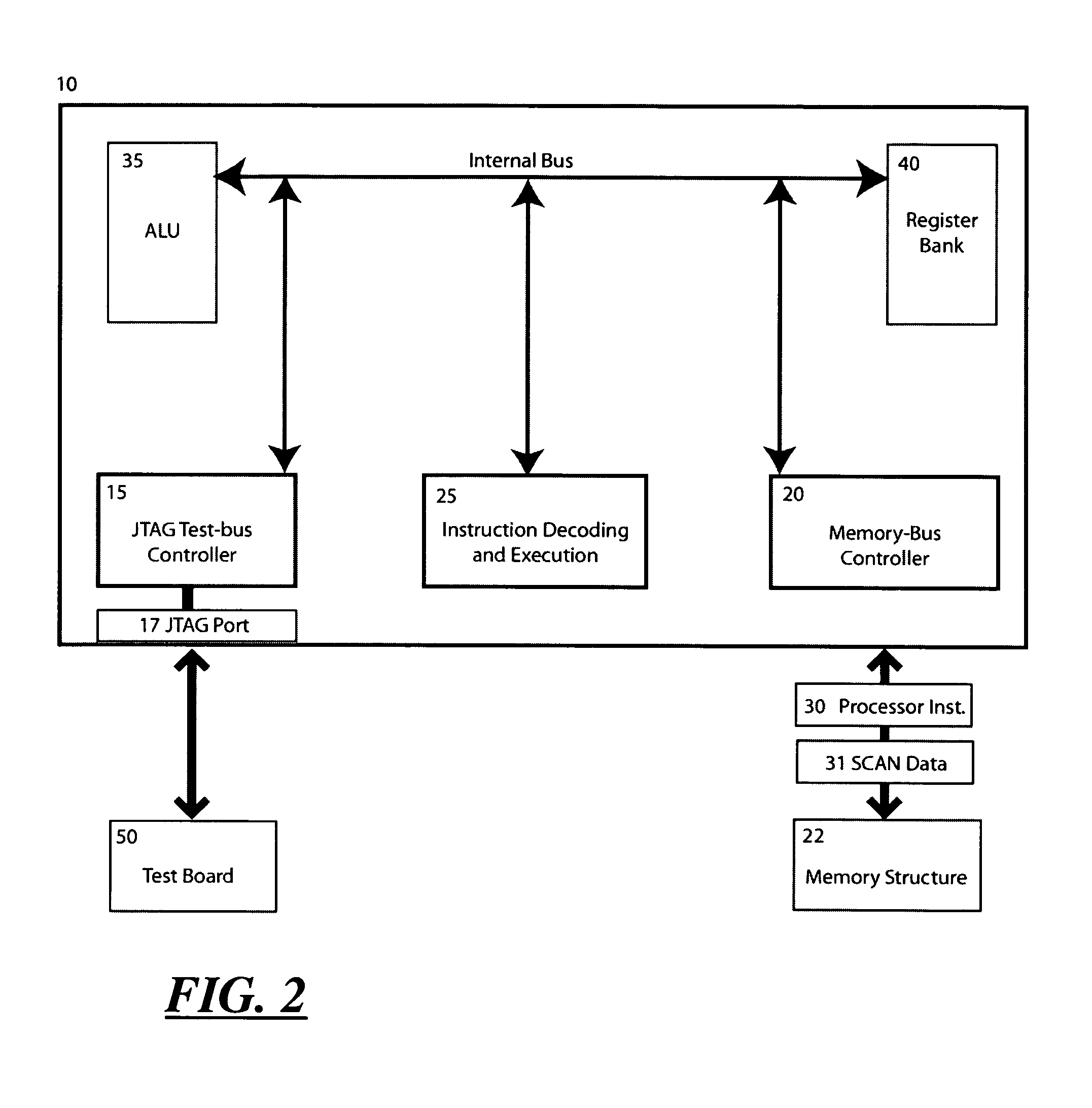
[0026]Referring to the accompanying FIG. 2, there is shown and described a test and debug processor 10 that can execute native test instructions. The processor 10 includes a JTAG-bus controller 15 with a JTAG port 17 coupled thereto, a memory means 20 or 22 capable of storing processor instructions 30 and scan data 31, and an instruction encoding unit 25 capable of fetching or requesting processor instructions from the memory means 20 or 22. The processor 10 may also include an optional ALU 35 and a memory-bus controller 48 connected to the JTAG-bus controller logic 15 making it a bus master. For example, in the case of a JTAG, the CPU can execute a SCAN_IR or SCAN_DR instruction directly after fetching it from memory. An example for such an instruction would be SIR R5, R6. This will let the CPU choose the SCAN_IR JTAG state and send all or part of the contents of register 5 (R5) to the test board. The data coming back from the test board will be stored in register 6 (R6). Another ...


PUM


Abstract

A test and debug processor capable of initiating, commanding and executing JTAG-bus functions without the involvement of an external CPU. The processor includes a JTAG-bus controller with a JTAG port coupled to it. The JTAG-bus functions are encoded in instructions and stored in a memory structure. The processor instructions are then fetched and executed directly by the JTAG-bus controller without software interpretation. The instructions optionally includes JTAG-bus end state, function duration information, information about the location of the data to be sent out to the test object and a location to store the information received from the test object. Optionally, the test and debug processor can directly access any memory structure to fetch or store test data objects by adding a memory bus-controller interface to the processor. The ability to execute arithmetic and logic operation and register transfer operations on test data can be added using an ALU.

Description

[0001]This application claims the benefit of U.S. Patent No. 60 / 324,240 filed on Sep. 21, 2001.BACKGROUND OF THE INVENTION[0002]1. Field of the Invention[0003]This invention pertains to electronic devices used to test and debug electrical circuits and, more particularly, such devices that use a Joint Test Action Group (JTAG) port.[0004]2. Description of the Related Art[0005]With the complexity and increase of pin-count of new computer chips and the dense assembly of these chips on circuit boards, it becomes increasingly difficult to test and debug the circuit boards after being assembled. A group of leading electronic companies has joined forces and developed a standard test port to be built on every chip. The purpose of this test port is to allow connection to a test tool to check the value of each pin on the chip. Some chips add more functionality to this test port to provide access to virtually any resource inside the chip. One example of an in situ test port is the “JTAG” (Joint...

Claims


Application Information

Patent Timeline
Patent Type & Authority Patents(United States)
IPC IPC(8): G06F11/00G06F11/36
CPCG06F11/2236
Inventor MICHAEL, SAM
Owner MICHAEL SAM
Why Eureka
Try Eureka