
Liquid crystal display panel

a liquid crystal display and panel technology, applied in non-linear optics, instruments, optics, etc., can solve the problems of limited view angle of conventional lcd, uneven display image, irregular shape, etc., and achieve simple and easy manufacturing process, avoid light leakage, and wide view angle

Active Publication Date: 2008-08-05
HANNSTAR DISPLAY CORPORATION
View PDF6 Cites 31 Cited by
  • Summary
  • Abstract
  • Description
  • Claims
  • Application Information

AI Technical Summary

Benefits of technology

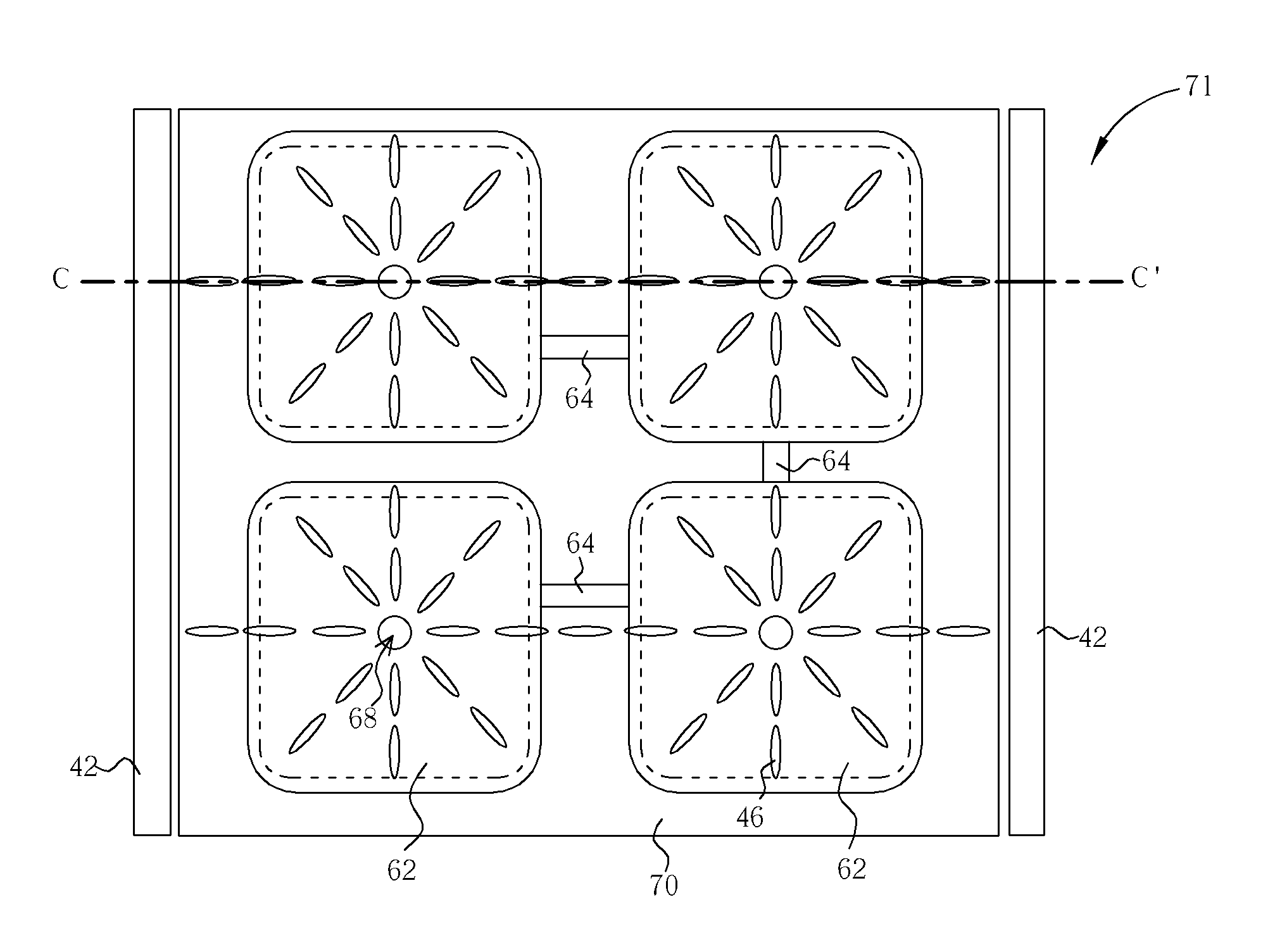
The present invention provides an LCD panel without protrusion that prevents light leakage and mura. The panel includes a common electrode on the first substrate, a liquid crystal layer with liquid crystal molecules and interposed between the first and second substrates, sub-pixel electrodes on the second substrate with an opening in the center, and patterned conductive layers functioning as bias electrodes around the sub-pixel electrodes. The sub-pixel electrodes and bias electrodes do not contact each other. The panel also uses a bias to achieve a wide view angle effect and avoids light leakage due to protrusion. The liquid crystal molecules at the edge portion of the sub-pixel electrode are aligned stably, reducing touch mura effect. The manufacturing process is simple and easy, and the display has a relatively high contrast ratio.

Problems solved by technology

However, the view angle of the conventional LCD is limited by the structure of the liquid crystal molecule and the optical character.
The alignment of liquid crystal is stable, but in the gray scale display, the display image is not uniform and irregular shapes appear.
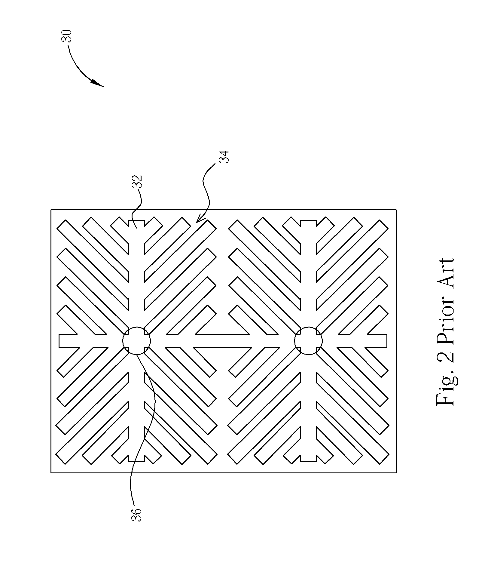
It is not easy to control the uniformity of the resist thickness during the manufacture, and accordingly the slit widths are not constant, such that an irregular shape of mura occurs when the display is operated.
Furthermore, the liquid crystal arrangement at the edge of the pixel in the vicinity of data lines is not stable, due to the electric field from the data lines.

Method used


Image

  • Liquid crystal display panel
  • Liquid crystal display panel
  • Liquid crystal display panel

Examples


Embodiment Construction

[0025]Please refer to FIGS. 3-9; the VALCD panel according to the present invention is described in detail hereinafter.

[0026]Please refer to FIG. 3 showing a schematic plan view of a LCD panel of one embodiment according to the present invention and FIG. 4 showing a cross-sectional schematic diagram of the LCD panel of FIG. 3 along the line BB′. The VALCD panel 40 according to the present invention comprises a first substrate 54 and a second substrate 56 disposed opposite each other. The material for substrate may be glass, quartz, or plastics. A common electrode 58 is disposed on the first substrate 54 on the side facing to the second substrate 56. A liquid crystal layer 46 comprising liquid crystal molecules is disposed between the common electrode 58 and the second substrate 56. A plurality of sub-pixel electrodes 52 are disposed between the surface of the second substrate at the side facing the first substrate 54 and the liquid crystal layer 46. Each sub-pixel electrode 52 has a...


PUM

PropertyMeasurementUnit
voltageaaaaaaaaaa
voltageaaaaaaaaaa
voltageaaaaaaaaaa

Abstract

A liquid crystal display panel is disclosed, in which each sub-pixel electrode has an opening in the center and a patterned conductive layer as a bias electrode is positioned relatively around the sub-pixel electrode. Upon being applied with a voltage, the liquid crystal molecules above the sub-pixel around the opening will tilt down outwardly and radially. Upon being applied with a bias voltage, the liquid crystal molecules above the bias electrode will be arranged parallel to the substrate due to the effect from the electric field. The liquid crystal layer may further comprise a chiral dopant, such that the molecules twist when they tilt.

Description

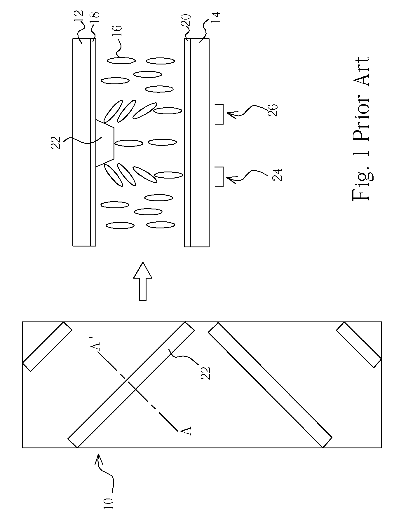
BACKGROUND OF INVENTION[0001]1. Field of the Invention[0002]The present invention relates to a liquid crystal display (LCD) panel, particularly a vertical alignment (VA) liquid crystal display panel, which does not include a protrusion and is accordingly without a light leakage occurring at an edge of the protrusion.[0003]2. Description of the Prior Art[0004]LCD devices have been widely used in various electronic devices, such as mobile phones, personal digital assistants (PDA), notebooks, terminals, television sets, becoming a main display product in the market. However, the view angle of the conventional LCD is limited by the structure of the liquid crystal molecule and the optical character. Thus, it is necessary to develop a LCD with wider view angle, such as a vertical alignment liquid crystal display (VALCD) panel.[0005]Please refer to FIG. 1, a schematic plan view of a conventional VALCD panel and a cross-sectional schematic diagram of the LCD panel along the line AA′. As sho...

Claims


Application Information

Patent Timeline
Patent Type & Authority Patents(United States)
IPC IPC(8): G02F1/1343G02F1/1337
CPCG02F1/134336G02F1/133707
Inventor SHIH, PO-SHENG
Owner HANNSTAR DISPLAY CORPORATION
Learn More